2025 Top PCB Components Trends and Innovations You Need to Know
In the rapidly evolving world of electronics, understanding the latest trends and innovations in PCB components is crucial for staying ahead of the competition. As we approach 2025, industry experts like Dr. Emily Chen, a leading engineer in PCB design, emphasize the importance of keeping abreast with emerging technologies. "The future of electronics heavily depends on the advancements in PCB components. They serve as the backbone of all digital devices, influencing performance and sustainability," she notes.
As we delve into the top PCB components trends and innovations that will shape the industry in the coming years, it is essential to recognize the increasing demand for miniaturization, higher performance, and improved efficiency. Today's designers are not just looking for traditional components but are seeking innovative solutions that integrate seamlessly into complex electronic systems. Understanding these trends will empower engineers and manufacturers alike to enhance their product offerings and meet the growing needs of consumers.
As we explore this dynamic field, we'll highlight key innovations in materials, design methodologies, and manufacturing processes, providing insights that are vital for anyone involved in the PCB components sector. The ability to adapt and innovate in response to these trends will not only redefine product capabilities but will also pave the way for groundbreaking applications in diverse industries.

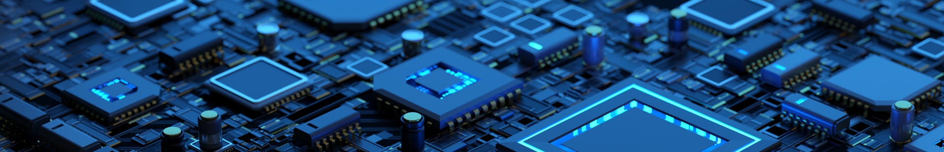
Key PCB Component Innovations Revolutionizing Electronics in 2025
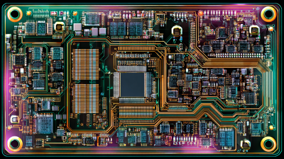
The landscape of PCB components is rapidly evolving, driven by innovative technologies that are set to revolutionize the electronics industry in 2025. One of the key trends is the integration of advanced materials that enhance performance and reduce size. For instance, the use of flexible and high-frequency laminate materials is gaining traction, allowing for more compact designs that can efficiently manage heat and improve signal integrity. This shift towards smaller, more powerful PCBs not only caters to the growing demand for miniaturization in electronic devices but also supports the advent of wearable technology and IoT applications.
Another significant innovation lies in the area of smart components, which incorporate sensors and processing capabilities directly into the PCB design. This not only simplifies the design process but also enables real-time data collection and analysis, paving the way for smarter systems. The integration of AI-driven components can optimize performance based on user interaction and environmental conditions, ultimately leading to more efficient and responsive electronic devices. As we look ahead, these advancements promise to define the future of electronics, making them more intelligent, compact, and environmentally friendly.
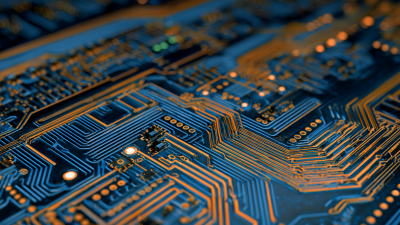
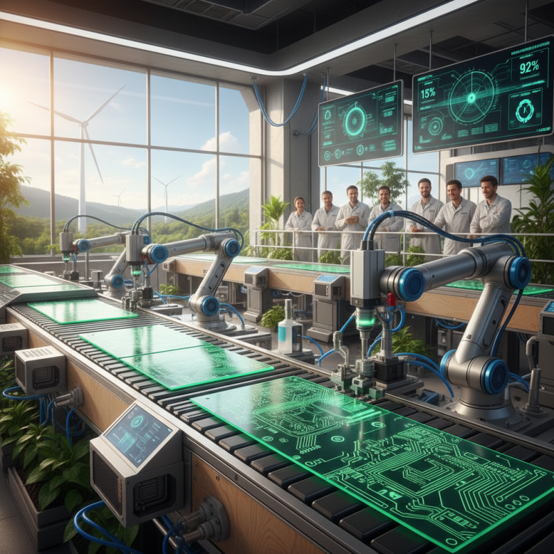
2025 Top PCB Components Trends and Innovations
This chart illustrates the predicted growth trends for various PCB components by 2025, highlighting the innovations poised to revolutionize the electronics industry.
Emerging Materials for PCB Manufacturing: Trends and Benefits in 2025
The landscape of PCB manufacturing is set to undergo significant transformations in 2025, driven largely by the emergence of innovative materials that promise enhanced performance and sustainability. One of the most notable trends is the use of advanced polymer composites, which offer superior electrical insulation and thermal stability. These materials not only improve the overall reliability of PCB designs but also support miniaturization efforts, enabling the development of more compact and efficient electronic devices.
Another compelling trend is the incorporation of biodegradable materials in PCB manufacturing processes. As environmental concerns continue to rise, manufacturers are increasingly looking to replace traditional materials with sustainable alternatives. These biodegradable options not only reduce environmental impact but also maintain the necessary performance standards for high-tech applications. By adopting such materials, companies can enhance their green credentials while meeting the demands for high-efficiency circuitry in various sectors, including consumer electronics and automotive industries.
2025 Top PCB Components Trends and Innovations You Need to Know - Emerging Materials for PCB Manufacturing: Trends and Benefits in 2025
| Component |
Material Type |
Key Trend |
Benefits |
| Flexible PCBs |
Copper Polyimide |
Increased Usage in Wearables |
Lightweight, Space-saving, High Flexibility |
| High-Frequency PCBs |
PTFE (Teflon) |
Growth in Telecommunications |
Low Loss, High Performance |
| Embedded Capacitor PCBs |
Ceramic Materials |
Miniaturization of Circuits |
Compact Design, Improved Functionality |
| Thermal Management Boards |
Thermal Conductive Materials |
Focus on Heat Dissipation |
Enhanced Performance, Reliability |
| High-Reliability PCBs |
Epoxy Resins |
Increasing Demand in Aerospace |
Durability, Strong Mechanical Properties |
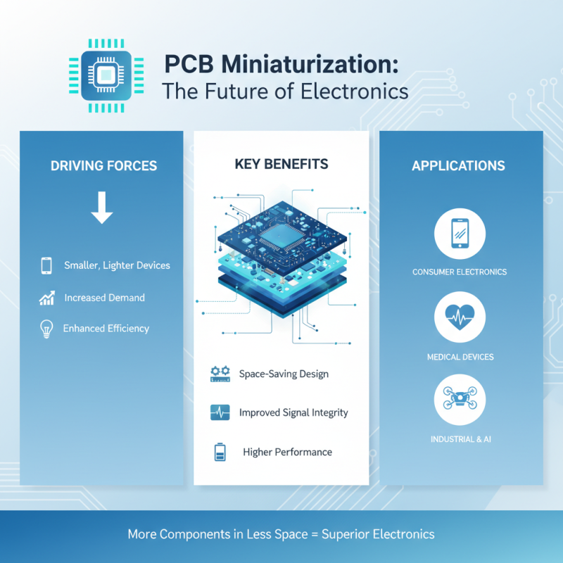
The Role of Miniaturization in Future PCB Design and Functionality
As technology advances, the role of miniaturization in PCB design becomes increasingly critical. The demand for smaller, lighter, and more efficient electronic devices drives engineers to adopt innovative design strategies that prioritize space-saving solutions. Miniaturization not only allows manufacturers to fit more components into compact spaces but also enhances performance by reducing the distances electrical signals must travel. Consequently, this leads to improvements in signal integrity and power efficiency, which are essential for high-performance applications ranging from consumer electronics to medical devices.
In the realm of future PCB functionality, miniaturization is intertwined with emerging technologies such as IoT devices, wearable technologies, and advanced communications systems. These applications require PCBs that are not only small but also capable of integrating various functions, such as sensing, processing, and connectivity, within a limited footprint. Innovations in materials and manufacturing processes, such as flexible PCBs and advanced substrates, enable designers to push the boundaries of size and performance. As we look ahead, the ability to create micro-sized components with enhanced capabilities will redefine product development and open new avenues for technological advancement across industries.
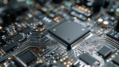
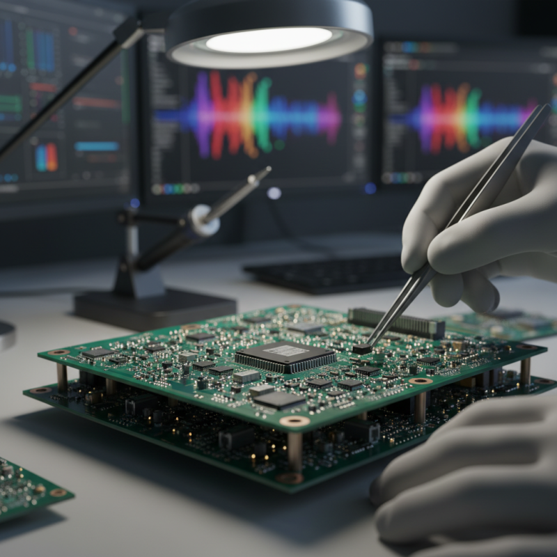
Advancements in PCB Assembly Techniques and Their Impact on Efficiency
The advancements in PCB assembly techniques have significantly impacted the efficiency and effectiveness of electronic manufacturing in recent years. As the demand for compact and high-performance devices continues to rise, manufacturers are increasingly adopting innovative techniques that streamline the assembly process. Among these advancements are automated assembly systems that utilize robotics and AI-driven technologies, drastically reducing assembly times while enhancing precision. This not only minimizes human error but also allows for intricate designs to be achieved more reliably.
Moreover, the introduction of solderless assembly methods and advanced adhesive technologies is transforming how components are integrated onto PCBs. These methods enable more flexible design choices and improve thermal management by reducing stress on components during the assembly process. As a result, manufacturers can produce more durable and efficient PCBs capable of supporting innovative applications in consumer electronics, automotive, and telecommunications. The synergistic effect of these advancements promises to drive further innovation in the industry, fostering an environment where efficiency and performance go hand in hand.
Sustainable Practices in PCB Production: Trends Shaping the Future
Sustainable practices have become integral to the printed circuit board (PCB) production industry as companies recognize the importance of environmental responsibility. According to a report by Research and Markets, the global green electronics market is projected to reach $1 trillion by 2025, emphasizing the demand for eco-friendly components and processes. PCB manufacturers are increasingly adopting sustainable materials, such as biodegradable substrates and lead-free solder, to reduce their environmental impact. Innovations in production techniques, including the use of water-based solvents and energy-efficient machinery, further drive sustainability in the sector.
Moreover, the shift towards circular economy principles is shaping the future of PCB production. The International Renewable Energy Agency (IRENA) highlights that recycling and recovering materials from end-of-life electronics not only minimizes waste but also significantly lowers the carbon footprint associated with new product manufacturing. As a result, many manufacturers are investing in research to develop closed-loop systems that enable the reuse of materials in PCB production, thus ensuring that sustainability becomes a core aspect of their operational strategy. The growing emphasis on these green practices will not only help companies comply with stricter regulations but also cater to the increasing consumer demand for environmentally-friendly products.