What is Altium PCB Design and How Can It Transform Your Electronics Projects
In the fast-evolving world of electronics, the demand for precision and efficiency in design has never been greater. Altium PCB Design stands at the forefront of this transformative wave, offering a robust platform that revolutionizes the way engineers and designers approach printed circuit board development. With its intuitive interface and powerful features, Altium PCB Design allows users to streamline their workflow, from initial concept to final production, empowering them to create innovative solutions that meet the complexities of modern electronics projects.
The integration of advanced design tools, coupled with real-time collaboration capabilities, enhances productivity and reduces the risk of errors, enabling teams to iterate quickly and effectively. By harnessing the power of Altium PCB Design, designers can achieve a level of precision that is crucial in today’s competitive market. This article delves into the key features of Altium PCB Design and illustrates how it can transform ideas into tangible products, showcasing its role as an indispensable asset in the electronics design landscape.

Understanding Altium PCB Design and Its Features
Altium PCB design is a powerful tool that has revolutionized the way engineers and designers approach electronics projects. At its core, Altium offers an integrated environment that combines schematic capture, PCB layout, and design validation in a seamless workflow. This means that users can create sophisticated electronic circuits with agility, ensuring that projects move from conception to production more efficiently. The intuitive interface enables even those who are new to PCB design to grasp the essentials quickly, allowing for creative exploration without steep learning curves.
One of the key features of Altium PCB design is its advanced simulation capabilities. These tools enable designers to test and validate their designs virtually, identifying potential issues before physical prototypes are created. Additionally, the platform supports a range of libraries and components, streamlining the design process and reducing the risks of errors. The collaborative features also allow teams to work together in real-time, facilitating communication and enhancing productivity. By leveraging Altium, designers can transform their electronics projects into robust, reliable, and innovative solutions tailored to meet the demands of modern technology.
The Importance of PCB Design in Electronics Projects
The importance of PCB design in electronics projects cannot be overstated. A well-designed printed circuit board (PCB) is crucial for the effective functioning of electronic devices. It serves as the backbone of electronic circuitry, connecting various components in an organized and efficient manner. With proper PCB design, engineers can ensure signal integrity, minimize electromagnetic interference, and enhance the overall reliability of the product. In rapidly evolving fields such as IoT and wearable technology, robust PCB design becomes even more essential to meet the demands for compactness and efficiency.
When approaching PCB design, it is vital to consider a few tips that can significantly improve the process. First, invest time in creating a detailed schematic before moving on to layout design. This foundational step helps in visualizing the interconnections between components and prevents potential errors in the design. Second, utilize design rule checks (DRC) to automatically identify any discrepancies or issues in the layout. This feature ensures that all electrical standards are met, leading to a smoother manufacturing process. Lastly, prototype your design before full-scale production. Testing a prototype helps in identifying and rectifying any flaws early on, ultimately saving time and resources.
By prioritizing effective PCB design, you can not only enhance the quality of your electronics projects but also ensure they are scalable, reliable, and ready for market demands. The integration of thoughtful design practices is what separates average projects from truly innovative solutions in today's technology landscape.
Key Benefits of Using Altium for PCB Design
Altium PCB design software offers several key benefits that can significantly enhance your electronics projects. One of the most compelling advantages is its unified environment, which integrates schematic capture, PCB layout, and embedded software development. This seamless integration allows for better collaboration among team members and minimizes the chances of errors that can arise from switching between different tools. By having everything in one platform, designers can easily iterate on their designs, ensuring greater efficiency and accuracy throughout the development process.
Another important benefit of using Altium for PCB design is its advanced design rule checking capabilities. This feature automatically verifies that your design adheres to specified electrical and manufacturing rules, helping to identify potential issues early in the design phase. Additionally, the robust simulation tools available within the platform allow for thorough testing of the PCB’s performance before production. This proactive approach not only saves time and reduces costs but also enhances the reliability of the final product, leading to successful outcomes in your electronics projects.
Step-by-Step Process of Designing a PCB with Altium
Designing a printed circuit board (PCB) with professional software can significantly enhance the precision and efficiency of electronics projects. The process typically begins with schematic capture, where you define the circuit’s functionality by placing and interconnecting components in a virtual environment. This initial step is crucial, as it sets the foundation for the layout and ensures that all necessary connections are correctly represented in the design.
Once the schematic is complete, the next phase involves transforming the schematic into a physical layout. This step entails placing components on the board and routing the electrical connections while adhering to design rules such as spacing and signal integrity. Effective component placement can influence not only performance but also manufacturability. After the layout is finalized, a design rule check (DRC) is performed to identify any potential issues, ensuring that the board meets the required specifications. Following this validation, the final output files are generated for fabrication, paving the way for prototype development and testing in your electronics projects.
What is Altium PCB Design and How Can It Transform Your Electronics Projects
| Step |
Description |
Tools Required |
Outcome |
| 1 |
Define project requirements and specifications. |
Requirements document, brainstorming sessions. |
Clear project scope. |
| 2 |
Create a schematic design. |
Altium Designer, component library. |
Functional schematic. |
| 3 |
Convert the schematic to PCB layout. |
Altium Designer, PCB library. |
Initial PCB layout. |
| 4 |
Place components and route the PCB. |
Altium Designer, auto-router tools. |
Completed PCB design. |
| 5 |
Run design rule checks and simulations. |
Altium Designer, simulation tools. |
Validated design. |
| 6 |
Generate manufacturing files. |
Altium Designer. |
Production-ready files. |
Real-World Applications of Altium in Electronics Development
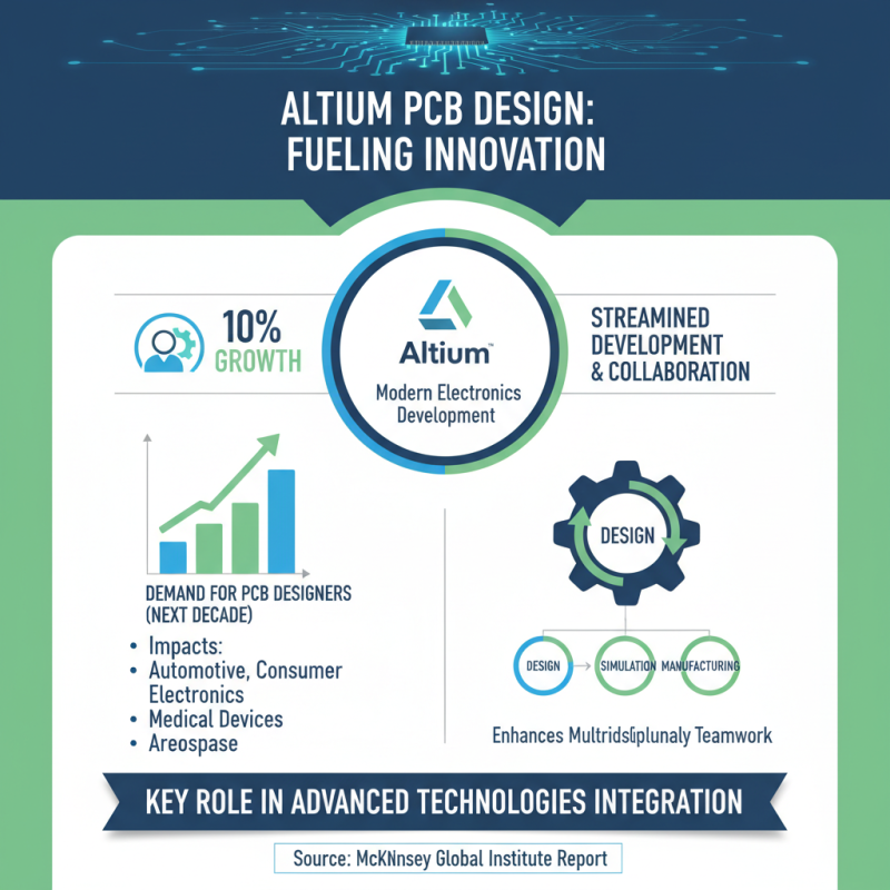
Altium PCB design plays a pivotal role in modern electronics development, significantly influencing various industries from automotive to consumer electronics. According to a report by the McKinsey Global Institute, the demand for PCB designers is expected to grow by 10% over the next decade as more companies integrate advanced technologies into their products. This trend highlights the necessity for robust design software that can streamline the development process and enhance collaboration among multidisciplinary teams.
One notable application of advanced PCB design is seen in the healthcare sector, where precision and reliability are paramount. For instance, medical devices, which increasingly rely on intricate electronic components, require PCBs that are not only efficient but also compliant with rigorous industry standards. A study by Research and Markets indicates that the global printed circuit board market in the medical field is projected to expand at a CAGR of 6.3%, underscoring the critical role of quality design in innovation. Altium facilitates such developments by providing integrated tools that allow engineers to rapidly prototype and iterate their designs, resulting in faster time-to-market for life-saving technologies.
In the automotive industry, the integration of electric and autonomous vehicles has further amplified the importance of high-quality PCB design. A recent analysis from the International Data Corporation (IDC) reveals that smart vehicle electronics will account for approximately 30% of total vehicle costs by 2030. This shift necessitates advanced design capabilities to manage the complex interconnectivity of components within these vehicles. Utilizing sophisticated PCB design software enables engineers to simulate their designs under various conditions, ensuring optimal performance and reliability as they revolutionize transportation.