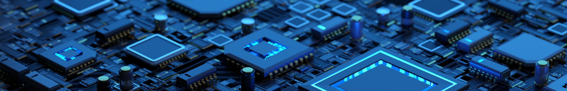
Top 10 Best Practices for Effective PCB Design in Electronics Engineering
In the rapidly evolving field of electronics engineering, the significance of effective PCB design cannot be overstated. As per the latest market insights from IPC's
“Global Market Study on the PCB Industry,” the demand for printed circuit boards (PCBs) is projected to exceed
$80 billion by 2025, driven primarily by advancements in telecommunications, automotive applications, and the Internet of Things (IoT).
This remarkable growth highlights the need for industry professionals to adopt best practices in PCB design to enhance performance, reduce costs, and ensure reliability.

Implementing best practices in PCB design is not just a technical necessity; it is a strategic imperative for maintaining competitiveness in the electronics sector.
According to a report by Mordor Intelligence, the PCB design software market is expected to grow at a compound annual growth rate
(CAGR) of over 9% from 2020 to 2025, indicating a rising focus on sophisticated design tools and methodologies.
As engineers navigate challenges such as miniaturization, thermal management, and signal integrity, understanding and applying
the top 10 best practices for effective PCB design will be crucial in creating innovative products that meet and exceed industry standards. Through this comprehensive approach,
firms can ensure their PCBs are not only functional but also optimized for the future.
Understanding the Fundamentals of PCB Design in Electronics Engineering
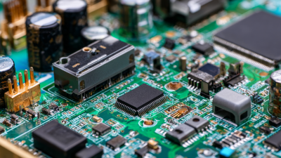
Understanding the fundamentals of printed circuit board (PCB) design is crucial in electronics engineering, as it serves as the backbone of electronic devices. According to a report by IPC, an international association for electronics manufacturing, over 70% of product failures are attributed to inadequate PCB design and fabrication processes. This highlights the necessity for engineers to adopt best practices that encompass a solid understanding of design principles and materials involved.
In electronics engineering, effective PCB design begins with thorough component placement and routing strategies. A study by Mentor Graphics indicates that 40% of designers underestimate the impact of layout decisions on signal integrity and electromagnetic compatibility. By incorporating simulation tools early in the design phase, engineers can anticipate potential issues, ensuring that the final product will meet performance specifications. Additionally, selecting appropriate materials tailored to the specific application can significantly enhance the reliability of the PCB, thereby reducing long-term operational costs.
Adopting these foundational practices is essential for any engineer looking to excel in the competitive field of electronics.

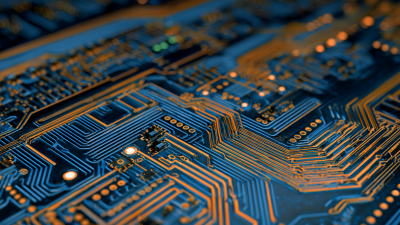
Key Considerations for Layer Stackup and Material Selection
In the realm of PCB design, the careful consideration of layer stackup and material selection is paramount for ensuring optimal performance and functionality. When planning the stackup, one must take into account the interconnect impedance, which is influenced by several variables such as trace width, copper thickness, dielectric thickness, and dielectric constant. Each of these factors plays a crucial role in determining how signals propagate through the PCB, directly affecting the overall system performance.
A well-designed stackup not only minimizes impedance mismatches but also addresses electromagnetic interference (EMI) concerns. The power distribution network (PDN) impedance, for example, is another critical aspect that directly impacts the device's resilience against noise. Selecting materials that offer the right balance between cost, longevity, and electrical properties ensures that the PCB design aligns with both performance and economic objectives. As the landscape of electronics engineering evolves, leveraging advanced planning tools can greatly enhance the precision and efficiency of stackup decisions.
Top 10 Best Practices for Effective PCB Design in Electronics Engineering - Key Considerations for Layer Stackup and Material Selection
| Best Practice |
Description |
Key Consideration |
Material Type |
| 1. Define Requirements |
Clear specifications for functionality, size, and frequency. |
Electrical Characteristics |
FR-4 |
| 2. Optimize Layer Stackup |
Minimize layers while ensuring signal integrity. |
Trace Impedance |
High-Speed Materials |
| 3. Use Via Options Wisely |
Select through-hole or blind/buried vias appropriately. |
Manufacturability |
Copper |
| 4. Pay Attention to Heat Management |
Design for adequate heat dissipation in high-power applications. |
Thermal Performance |
Thermal Pads |
| 5. Implement Signal Integrity Techniques |
Use techniques like differential pair routing. |
Noise Reduction |
Low-loss Dielectric |
| 6. Select Suitable Materials |
Choose based on frequency, temperature, and mechanical properties. |
Material Properties |
Composite Materials |
| 7. Emphasize Grounding Strategy |
Use ground planes effectively to reduce EMI. |
Electromagnetic Shielding |
Solid Copper |
| 8. Follow Design Rules |
Adhere to manufacturer and industry design guidelines. |
Compliance Standards |
Industry Standards |
| 9. Review Design for DFM and DFA |
Ensure the design is manufacturable and assemblable. |
Cost Efficiency |
Standard Materials |
| 10. Prototype and Test |
Build prototypes and conduct thorough testing. |
Validation |
Test Materials |
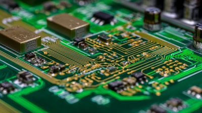
Strategies for Effective Component Placement and Routing Techniques
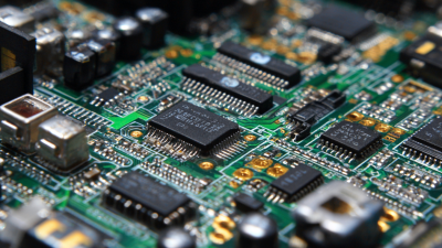
Effective component placement and routing techniques are crucial for optimizing PCB design within electronics engineering. According to a report from IPC, about 70% of PCB failures are related to poor design practices, emphasizing the importance of thoughtful placement and routing. A well-structured layout minimizes signal interference, enhances thermal performance, and improves manufacturability. Placing components in a logical sequence, based on the signal flow, can significantly reduce trace lengths, thereby diminishing the risk of electromagnetic interference (EMI).
Furthermore, advanced routing strategies, such as differential pair routing and impedance matching, play a vital role in high-speed PCB designs. Research from Mentor Graphics indicates that designs incorporating these strategies can achieve up to 25% improvement in signal integrity. Utilizing tools like autorouters with manual tweaks allows engineers to create efficient pathways while ensuring that power and ground planes are optimally utilized. This tiered approach not only streamlines the design process but also adheres to high industry standards for performance and reliability.
The Importance of EMI/EMC Considerations in PCB Design
In contemporary PCB design, the significance of addressing
Electromagnetic Interference (EMI) and
Electromagnetic Compatibility (EMC) cannot be overstated.
As electronic devices become more sophisticated and densely packed, the risk of EMI increases, potentially disrupting the performance of sensitive circuits.
A recent report highlighted that poor EMI performance is responsible for nearly 30% of project delays in electronic design.
This underscores the necessity for designer vigilance and the implementation of effective EMI mitigation strategies from the earliest stages of design.
Furthermore, the integration of system-level signal integrity analysis tools into PCB design highlights the evolving landscape of electronic engineering.
These methodologies are not only crucial for ensuring signal fidelity in traditional designs but are now being adapted for chiplet architectures,
which demand heightened signal integrity due to their unique interconnect challenges.
As Kush Desai points out, the demand for high-speed and low-power hardware emphasizes the need for refined design processes that prioritize
EMI shielding and power integrity.
Implementing proper shielding techniques and optimizing layout configurations can significantly reduce EMI, allowing systems to operate efficiently under the increasing load-power requirements of modern applications.
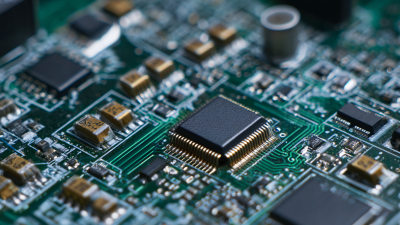
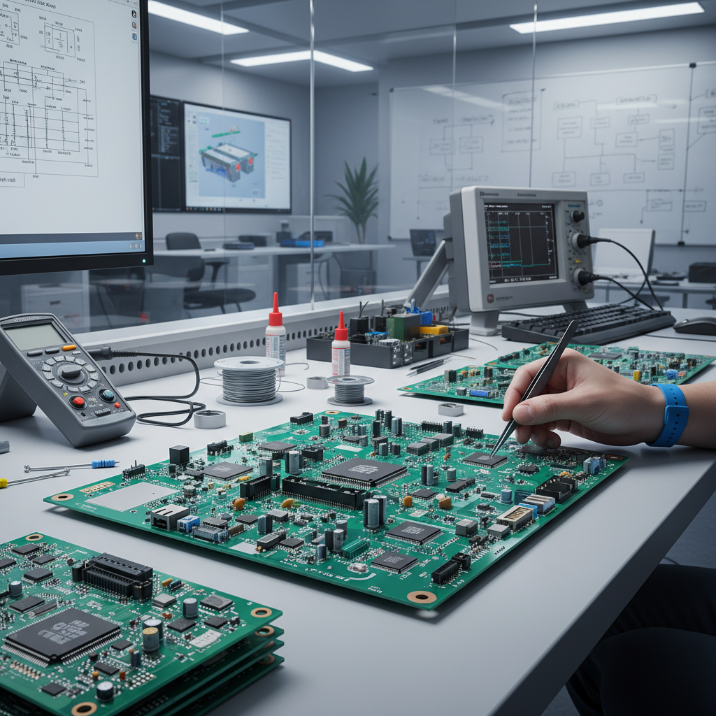
Optimizing Design for Manufacturability and Testing Efficiency
In the realm of electronics engineering, optimizing design for manufacturability (DFM) and testing efficiency is paramount for producing reliable printed circuit boards (PCBs).
DFM strategies begin with selecting components that are readily available and financially feasible, ensuring that the cost of production stays manageable while minimizing lead times.
Simplifying the PCB layout is also crucial; a clear and concise design reduces the complexity of manufacturing processes, which can diminish the likelihood of errors and defects during assembly.
Additionally, strategic placement of components promotes better thermal management and simplifies the soldering process.
Testing efficiency is equally important and should be integrated into the design phase.
Employing design for testability (DFT) principles allows engineers to identify potential faults early in the process.
This can include incorporating test pads and optimizing the arrangement of components to facilitate accessibility for probes and fixtures.
Furthermore, using simulation software to model circuit behavior helps in detecting issues before physical prototyping, thereby streamlining the testing phase.
By focusing on DFM and testing efficiency, engineers can enhance the overall performance and reliability of PCBs while reducing time-to-market and associated costs.