How to Choose the Right PCB Fabrication Process for Your Project
In the ever-evolving landscape of electronics manufacturing, selecting the appropriate PCB (Printed Circuit Board) fabrication process is crucial for the success of any project. As highlighted in the 2022 IPC Market Research report, the global PCB industry reached a valuation of approximately $70 billion, and this number is projected to grow at a compound annual growth rate (CAGR) of 3.8% over the next five years. This growth underscores the increasing demand for efficient, high-quality PCB fabrication techniques tailored to diverse applications ranging from consumer electronics to industrial systems.
Choosing the right PCB fabrication process is not merely a technical decision; it significantly impacts product performance, manufacturing costs, and time-to-market. The latest industry insights reveal that manufacturers must navigate a plethora of methods, including standard FR-4 processes, advanced materials for high-frequency applications, and bespoke fabrication techniques for specialized requirements. Moreover, according to the Smithers Pira report, the shift toward miniaturization and complexity in electronic devices necessitates a deeper understanding of the materials and processes involved in PCB fabrication, emphasizing the need for well-informed decision-making based on specific project needs and industry benchmarks.

Understanding PCB Fabrication Types and Their Applications
When selecting a PCB fabrication process, understanding the different types of PCB fabrication methods and their applications is crucial for achieving project goals. The most common types include single-sided, double-sided, and multi-layer PCBs. Single-sided PCBs are ideal for simpler electronics where space is limited, offering cost-effectiveness and ease of production. Double-sided PCBs allow for more complex circuit designs by utilizing both sides of the board, making them suitable for medium-complexity applications such as consumer electronics and industrial machinery.
Multi-layer PCBs, on the other hand, are essential for high-density applications requiring advanced electrical performance and miniaturization. They consist of multiple layers of circuitry and insulation, allowing for intricate designs that support advanced functions in telecommunications and high-speed computing devices. Each fabrication type comes with specific design considerations, such as layer count, trace width, and material selection, which directly influence the board's performance and durability according to the project's unique requirements. Understanding these applications can help ensure the right choice aligns with the intended use and technical specifications of the project.
How to Choose the Right PCB Fabrication Process for Your Project
| PCB Fabrication Type |
Material Used |
Layer Count |
Typical Applications |
Cost |
| Single-Sided PCB |
FR-4 |
1 |
Consumer Electronics, Toys |
Low |
| Double-Sided PCB |
FR-4 |
2 |
Home Appliances, Automation |
Medium |
| Multi-Layer PCB |
FR-4 / Polyimide |
3 to 10+ |
Computers, Medical Devices |
High |
| Rigid PCB |
FR-4, Aluminum |
1 or more |
LED Lighting, Industrial Equipment |
Medium to High |
| Flexible PCB |
Polyimide |
1 to 6 |
Wearable Devices, Medical Sensors |
Medium |
| Rigid-Flex PCB |
FR-4 and Polyimide |
Varies |
High-Tech Devices, Aerospace |
High |
Key Factors to Consider in PCB Material Selection
When selecting materials for printed circuit boards (PCBs), several key factors come into play that can significantly affect the performance and reliability of the final product. The first consideration is the thermal properties of the material. Depending on the application, the PCB may need to withstand high temperatures during operation or manufacturing processes. Materials with good thermal conductivity, such as FR-4 for standard applications or more specialized substrates for high-performance scenarios, can enhance heat dissipation and ensure circuit integrity under various conditions.
Another important factor is the dielectric constant of the materials used. This property affects signal integrity, especially in high-frequency applications. Variations in the dielectric constant can lead to signal loss or distortion, making it crucial to select materials that maintain consistent electrical performance across the desired frequency range. Additionally, mechanical properties, including flexibility and strength, should also be considered, particularly for PCBs in wearable or portable devices where durability and resistance to bending are necessary. Selecting the right combination of these material properties will ultimately influence the effectiveness and longevity of the PCB in its intended application.
Key Factors in PCB Material Selection
Evaluating Design Complexity and Its Impact on Fabrication Process
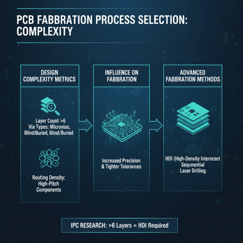
When choosing the right PCB fabrication process, assessing the complexity of your design is crucial. Research shows that PCB complexity metrics, such as layer count, via types, and routing density, significantly influence the selection of fabrication methods. For example, a study by the IPC (Institute of Printed Circuits) indicates that designs with more than six layers require advanced fabrication techniques like HDI (High-Density Interconnect) to achieve the necessary performance and reliability. As designs increase in intricacy, the need for precision and fine-pitch components grows, demanding processes that can accommodate tighter tolerances and finer features.
Additionally, fabrication capabilities directly correlate with design requirements; complex PCBs often lead to increased manufacturing costs and longer lead times. According to a report by the IPC Market Research, projects with mixed technology designs, which incorporate both surface mount and through-hole components, saw a 20% increase in overall fabrication costs compared to simpler designs. This underscores the importance of thoroughly understanding design complexity during the planning phase. Ultimately, choosing a fabrication process that aligns with your project's complexity ensures efficient production and optimal functionality while mitigating the risk of unforeseen delays and budget overruns.
Cost Analysis: Balancing Quality and Budget in PCB Production
When embarking on a PCB fabrication project, balancing quality with cost is paramount. The production process can vary significantly in price depending on the materials, technology, and design complexity involved. A thorough cost analysis should include not only the base price of manufacturing but also considerations such as turnaround time, testing, and potential rework. Often, opting for lower-cost materials may save money upfront but can lead to higher failure rates and increased long-term costs.
To optimize your budget while ensuring quality, it is essential to evaluate the specific requirements of your project. High-density interconnect (HDI) boards may offer superior performance and miniaturization, but they typically come with a higher price tag. Conversely, simpler designs could utilize standard fabrication techniques that are more cost-effective. Engaging with fabrication partners who provide transparent quotes and detailed breakdowns of costs can also lead to better budgeting decisions. In this way, you can strike the right balance between quality and cost, ensuring that your project meets both performance standards and financial constraints.
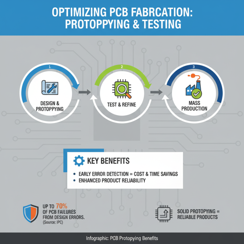
Implementing Prototyping and Testing in PCB Fabrication Choices
When choosing a PCB fabrication process, implementing effective prototyping and testing methods is critical. Prototyping allows engineers to identify and rectify design flaws before mass production, saving both time and resources. According to the IPC (Institute of Printed Circuits), up to 70% of PCB failures can be traced back to early design errors. Therefore, investing in a solid prototyping phase can significantly enhance the reliability of the final product.
When it comes to testing, incorporating various strategies such as Functional Testing (FT) and Automated Optical Inspection (AOI) helps ensure that each board meets the necessary specifications. Reports indicate that projects that implement comprehensive testing during the PCB fabrication process can reduce field failures by as much as 50%. The choice of testing methods should be tailored to the specific requirements of your project, considering factors like complexity, size, and end-use applications.
Tips: Start with a low-fidelity prototype to quickly iterate on initial design ideas without significant cost. Once the design is more refined, move to higher-fidelity prototypes to conduct detailed testing. Additionally, collaborate closely with your PCB manufacturer to leverage their insights on prototyping and testing capabilities that align with your project's needs. This partnership can lead to improved outcomes and more effective production cycles.