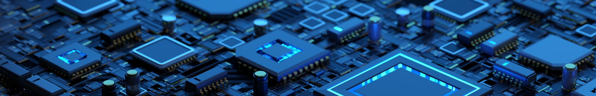
Understanding the Essential Steps in PCB Manufacturing and Assembly for Electronics Design
In the rapidly evolving landscape of electronics design, the significance of efficient PCB manufacturing and assembly cannot be overstated. According to a recent report from IPC, the global PCB market is projected to reach $100 billion by 2025, fueled by innovations in technology and increased demand for electronic devices across various sectors. This underscores the critical role that optimizing PCB manufacturing and assembly processes plays in ensuring product reliability, performance, and cost-effectiveness.
 As designers face the challenge of integrating more complex circuits while adhering to tighter timelines and budgets, understanding the essential steps in PCB manufacturing and assembly becomes paramount. These steps not only streamline the production process but also enhance the ability to respond to market trends and consumer needs. Therefore, this article delves into the key elements involved in PCB manufacturing and assembly, providing insights that are crucial for driving successful electronics design forward.
Key Stages in the PCB Manufacturing Process for Electronics Design
The PCB manufacturing process is critical to the success of electronics design, encompassing several key stages that ensure the product meets both technical and functional specifications. A thorough understanding of these stages—from design, prototyping, and fabrication to assembly and testing—enables designers to optimize their workflows and make informed decisions. Recent developments in the industry, such as new acquisitions and innovative software solutions, highlight the importance of integrating advanced technologies throughout the PCB manufacturing process.
For instance, a recent acquisition has expanded the capabilities of PCB design solutions, particularly for small and medium-sized businesses. This integration supports a seamless transition from design to manufacturing, illustrating the necessity of cohesive workflows in today's fast-paced electronics market. Additionally, the launch of new electronic design automation software promises significant improvements in performance and development speed, showcasing how modern tools can greatly enhance PCB design and manufacturing readiness. These advancements are crucial in addressing the increasing complexity of electronic products and ensuring that they meet global standards in functionality and reliability.
Understanding the Essential Steps in PCB Manufacturing and Assembly for Electronics Design
| Step |
Description |
Duration |
Key Considerations |
| Design Layout |
Create a schematic diagram and PCB layout. |
1-2 weeks |
Component placement, signal integrity, thermal management |
| Gerber File Generation |
Export design files in Gerber format for manufacturing. |
1 day |
Verify file accuracy and completeness |
| PCB Fabrication |
Manufacture the PCB using processes such as etching and plating. |
2-3 weeks |
Material selection, layer count, surface finish |
| Component Sourcing |
Identify and order necessary components for assembly. |
1-2 weeks |
Lead times, availability, cost-effectiveness |
| Assembly Process |
Assemble components onto the fabricated PCB. |
1-2 weeks |
Soldering methods, quality control, testing |
| Testing |
Perform functional and stress tests to ensure reliability. |
1 week |
Test plans, troubleshooting, documentation |
| Delivery |
Ship final products to customers. |
1 week |
Packaging, logistics, customer communication |
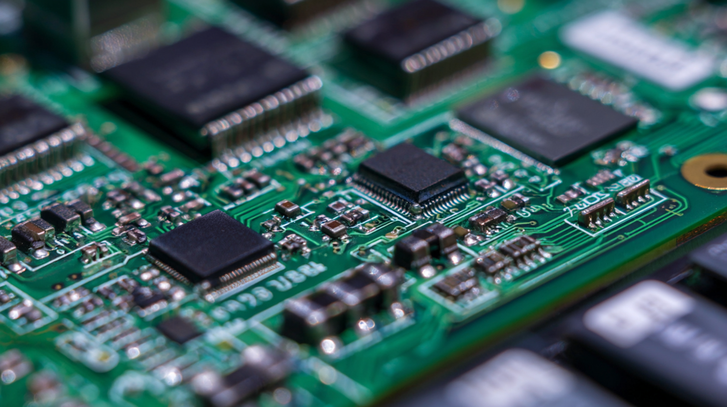
Essential Materials and Components Used in PCB Production
The manufacturing of printed circuit boards (PCBs) is a critical process in electronics design, relying heavily on specific materials and components to ensure optimal functionality and reliability. Key materials include substrates like FR-4, a fiberglass-reinforced epoxy resin that accounts for approximately 70% of the material used in PCB construction due to its excellent thermal and electrical insulation properties. According to a report by Market Research Future, the global PCB market is expected to grow at a CAGR of 3.6%, with the rising demand for high-tech applications such as IoT devices further driving the need for advanced materials.
Conductive materials are another essential component in PCB production, primarily copper, which is employed for circuit traces due to its superior conductivity. The average copper thickness in PCBs varies but typically ranges from 1 oz/ft² to 2 oz/ft², depending on the application. Additionally, solder mask and silkscreen inks are vital for protection and labeling, respectively, and are made from polymer-based solutions that enhance durability. The IPC, a global trade association, estimates that improper material selection can lead to significant quality issues, underscoring the importance of selecting the right components in the manufacturing process.
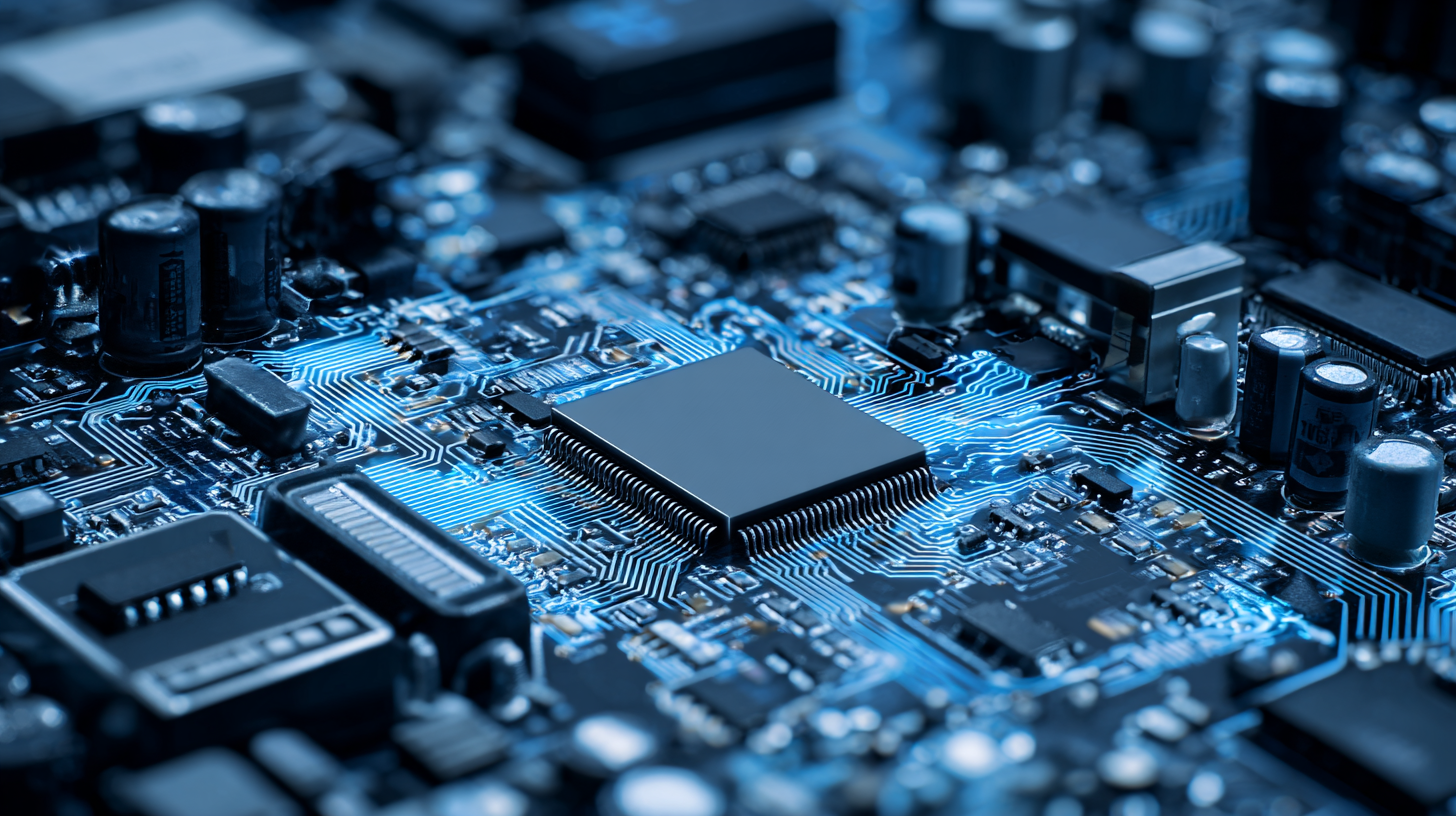
Best Practices for PCB Layout and Design Efficiency
Efficient PCB layout and design are critical for the successful manufacturing and performance of electronic devices. To start with, adopting a modular design approach can significantly enhance layout efficiency. By creating standardized modules that can be reused across different projects, designers can reduce development time and minimize errors. This method not only streamlines the design process but also leads to improved reliability and performance, as tested modules are often more dependable than custom-built solutions.
Another best practice is to prioritize signal integrity during the design phase. This involves carefully considering trace widths, lengths, and routing to minimize electromagnetic interference and crosstalk. Implementing controlled impedance techniques, such as maintaining consistent trace width and separation, can help achieve optimal communication between components. Additionally, using dedicated ground planes and strategically placing decoupling capacitors can further enhance signal stability, which is crucial for high-speed applications. By focusing on these aspects of layout design, engineers can create more efficient, reliable PCBs that meet the demands of modern electronics.
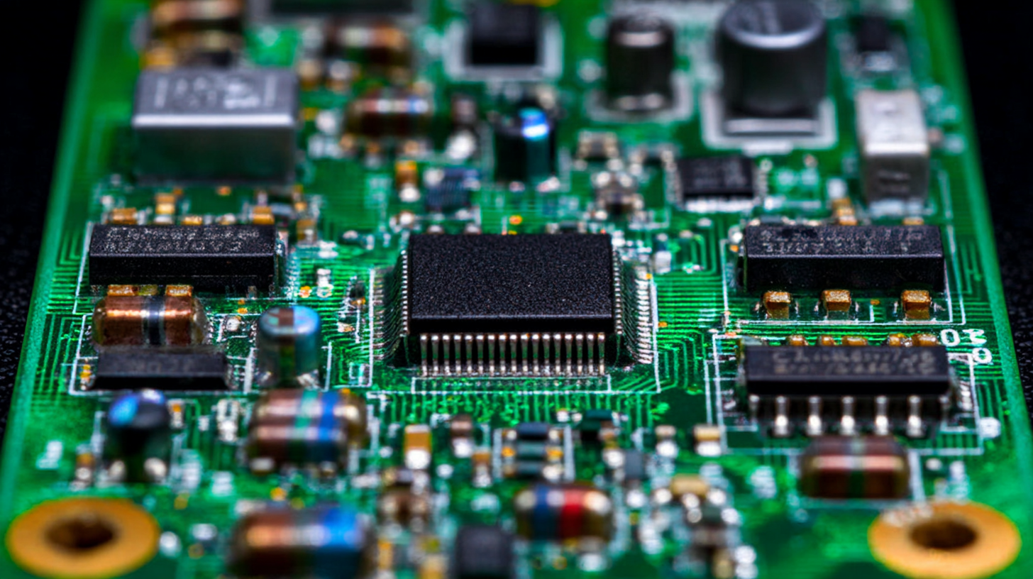
Techniques for Quality Control and Testing in PCB Assembly
Quality control and testing in PCB assembly are crucial steps that ensure the longevity and reliability of electronic devices. According to a report by IPC, nearly 80% of PCB manufacturing defects stem from the assembly phase. To mitigate these risks, employing advanced testing techniques such as Automated Optical Inspection (AOI) and X-ray inspection is essential. AOI allows manufacturers to detect visible defects like solder joint integrity and component placement, while X-ray inspection is effective for identifying hidden defects in multilayer boards.
Tips: Implementing a rigorous testing schedule throughout the PCB assembly process can significantly improve product reliability. Regular audits can help catch issues early, keeping defect rates below the industry standard of 3%.
Moreover, utilizing statistical process control (SPC) techniques plays a vital role in maintaining quality during assembly. This approach involves monitoring the manufacturing process through data collection and analysis, allowing for real-time adjustments that can prevent defects. A study by the International Electrotechnical Commission suggests that manufacturers using SPC techniques can reduce their defect rates by up to 50%, thus ensuring higher quality and consistency in their PCB products.
Challenges in PCB Manufacturing and Solutions for Electronics Design
The landscape of PCB manufacturing is rife with challenges that developers face in the electronics design process. As technology continues to advance, there are increasing demands for faster production times, higher precision, and cost-effectiveness. For instance, the rise of ultra-thin flexible PCBs showcases a significant shift toward innovative designs that require specialized manufacturing techniques. Addressing these challenges necessitates the integration of advanced technologies and methodologies, including AI-driven solutions that enhance design and production efficiency.
Moreover, industries are witnessing transformational changes due to emerging trends such as the adoption of AI in PCB fabrication. This technology streamlines workflows, optimizes designs, and significantly reduces the likelihood of errors throughout the manufacturing process. As the global PCB design software market is projected to grow substantially, companies need to embrace these advancements to stay competitive. Engaging in initiatives like the Bright Manufacturing Student Challenge not only fosters innovation but also equips future engineers with the skills needed to tackle the complex hurdles present in electronics design.
Challenges in PCB Manufacturing and Solutions for Electronics Design