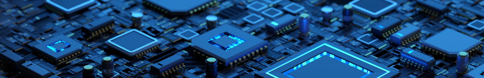
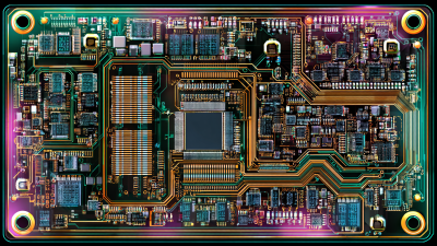
Ultimate Guide to Mastering PCB Board Design for Beginners and Experts
In the rapidly evolving electronics industry, mastering PCB board design has become increasingly essential for both beginners and seasoned professionals. According to a recent report by the IPC, the global PCB market is expected to reach $100 billion by 2025, reflecting a compound annual growth rate (CAGR) of 3.8%. This growth is driven by the rising demand in consumer electronics, telecommunications, and automotive sectors, where efficient and innovative PCB designs play a critical role. As a result, acquiring robust skills in PCB board design not only enhances a designer's capabilities but also significantly impacts the overall performance and reliability of electronic devices.

The importance of effective PCB board design cannot be overstated. A well-designed PCB minimizes electrical noise, optimizes signal integrity, and enhances the manufacturability of electronic products. Furthermore, the increasing complexity of circuits demands a thorough understanding of design practices and tools, as highlighted in the latest study by ResearchAndMarkets, which emphasizes that nearly 60% of engineering time is spent on design-related tasks. As such, this ultimate guide aims to equip designers with the knowledge and skills needed to navigate the intricacies of PCB board design, regardless of their experience level, ensuring they remain competitive in this dynamic field.
Understanding the PCB Design Process: From Concept to Prototype
Mastering the PCB design process is essential for both beginners and experienced engineers. It involves a comprehensive understanding of moving from concept to prototype, which has become significantly streamlined with the latest advancements in design software. For instance, recent innovations such as the release of a new version of a leading power design software have simplified power design tasks. This software version enhances efficiency by integrating advanced features tailored to meet modern design challenges, demonstrating a critical evolution in the PCB design landscape.
Moreover, the introduction of programmable logic devices that can encapsulate multiple functionalities into a single component is revolutionizing how engineers approach PCB design. This technology promises to minimize board size by up to 94% compared to traditional discrete logic implementations, facilitating faster prototyping and allowing for a more agile response to iterative design requirements. According to industry reports, such advancements in design automation tools are paving the way for a new era of electronic development, making the transition from idea to prototype faster and more efficient than ever before.
Essential Software Tools for PCB Design: Comparing Popular Options on the Market
When it comes to PCB design, choosing the right software tool is crucial for both beginners and seasoned professionals. There are a variety of options available in the market, each offering unique features tailored to different needs. Popular choices include Altium Designer, Eagle, and KiCad, each providing robust functionalities that can streamline the design process. Altium Designer is known for its user-friendly interface and powerful design capabilities, making it ideal for complex projects. In contrast, Eagle is favored for its affordability and is particularly suited for hobbyists and startups. KiCad stands out as a free, open-source tool, providing a comprehensive suite of tools for eager learners.
The differences between these software tools extend beyond price and complexity. Altium Designer excels in integration, allowing seamless collaboration with other design tools and comprehensive libraries. Eagle, with its cloud-related features, offers excellent sharing capabilities among team members, while KiCad benefits from a growing community that contributes libraries and support. Understanding these distinctions is fundamental for selecting the right PCB design software that aligns with your specific requirements, whether you are just starting out or looking to refine your existing skills.
Ultimate Guide to Mastering PCB Board Design for Beginners and Experts - Essential Software Tools for PCB Design: Comparing Popular Options on the Market
| Software Tool |
User Level |
Key Features |
Platform |
Pricing |
| Tool A |
Beginner |
User-friendly interface, basic design tools |
Windows, Mac |
Free / Basic Plan |
| Tool B |
Intermediate |
Advanced simulation, extensive libraries |
Windows |
$150/month |
| Tool C |
Expert |
High-performance features, collaboration tools |
Cloud-based |
$500/year |
| Tool D |
Intermediate |
3D modeling, extensive file support |
Windows, Linux |
$200/one-time |
| Tool E |
Beginner to Intermediate |
Drag-and-drop interface, real-time collaboration |
Web-based |
$10/month |
Key Design Principles and Rules for Effective PCB Layout Optimization
When embarking on PCB (Printed Circuit Board) design, understanding key design principles is crucial for both beginners and experts. One of the fundamental rules is to maintain a clear hierarchy of layers and components, which facilitates signal integrity and reduces noise. Placing critical components, such as decoupling capacitors, close to their respective ICs minimizes inductance and enhances performance. A clean and organized layout not only helps in troubleshooting but also eases the manufacturing process, ensuring consistent quality and reliability.
Another essential aspect of effective PCB layout optimization involves routing techniques. Designers should prioritize short, direct traces to enhance signal speed and reduce latency. Additionally, considering trace width and spacing according to current carrying capacity and electrical standards ensures that the board can handle required loads without overheating. Ground planes play a significant role in providing a low-resistance path and minimizing electromagnetic interference. By adhering to these principles, designers can create PCBs that are both efficient and effective, catering to the specific needs of the project while adhering to industry standards.
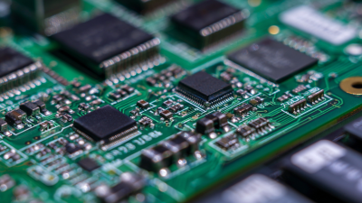
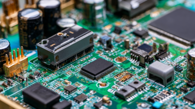
Common Manufacturing Techniques and Their Impact on PCB Performance
When it comes to PCB board design, understanding the common manufacturing techniques is crucial for optimizing both functionality and performance. Techniques such as surface mount technology (SMT) and through-hole technology (THT) each bring distinct advantages and limitations.
SMT, for instance, allows for a more compact design due to the smaller size of components, which can lead to improved electrical performance by reducing signal path lengths. Conversely, THT can provide stronger mechanical connections, which may be beneficial for devices requiring higher durability.
Additionally, the choice of materials and fabrication processes greatly influences PCB performance. For example, the use of high-frequency laminate materials can enhance signal integrity in high-speed applications, while the choice of surface finishes—like ENIG or HASL—can affect solderability and long-term reliability. Understanding these manufacturing techniques and their implications enables both beginners and experts to make informed decisions, ultimately leading to more efficient and reliable PCB designs tailored to specific applications.
Prototyping Techniques: Evaluating Costs and Benefits in PCB Development
Prototyping is a crucial step in PCB development that allows designers to evaluate the practicality of their designs before moving into large-scale production. By creating prototypes, engineers can identify potential issues such as layout flaws, component placement challenges, or signal integrity problems. This iterative process not only aids in refining the design but also significantly reduces the risk of costly errors down the line. Additionally, prototyping enables the assessment of different manufacturing techniques, helping teams choose the most cost-effective solution tailored to their project requirements.
Cost considerations in prototyping can vary widely based on materials, complexity, and the chosen fabrication methods. While rapid prototyping techniques may incur a higher upfront cost, they can lead to substantial savings by shortening the development timeline and reducing the likelihood of design revisions. Conversely, traditional methods might offer lower costs initially but could prolong the developmental cycle if significant design changes are needed. Striking the right balance between cost and efficiency in prototyping is essential for successful PCB development and can ultimately determine the project's overall success.