2025 How to Master PCB Design Techniques for Beginners and Professionals
In the rapidly evolving field of electronics, mastering PCB design techniques is essential for both beginners and professionals. As the technology matures, designers face new challenges and opportunities that demand a robust understanding of various design principles and best practices.
Renowned PCB design expert Dr. Jane Smith once stated,
"Innovation in PCB design is not just about creating circuits; it's about realizing the full potential of technologies for a smarter future."
This insight highlights the significance of honing skills that will not only enhance individual projects but also contribute to advancements in the industry.
As we approach 2025, the demand for expertly designed printed circuit boards (PCBs) continues to surge, making it crucial for aspiring designers to keep pace with the latest techniques. Whether one is just starting out or looking to refine existing skills, understanding the fundamentals and emerging trends in PCB design can pave the way for success.
This article outlines the top 10 techniques and strategies that will empower designers at all levels to excel in their PCB design endeavors, ensuring they are well-equipped to tackle the complexities of modern electronics.
Embrace the challenge and prepare to elevate your PCB design skills to new heights.
Understanding the Basics of PCB Design: Essential Concepts for All Levels
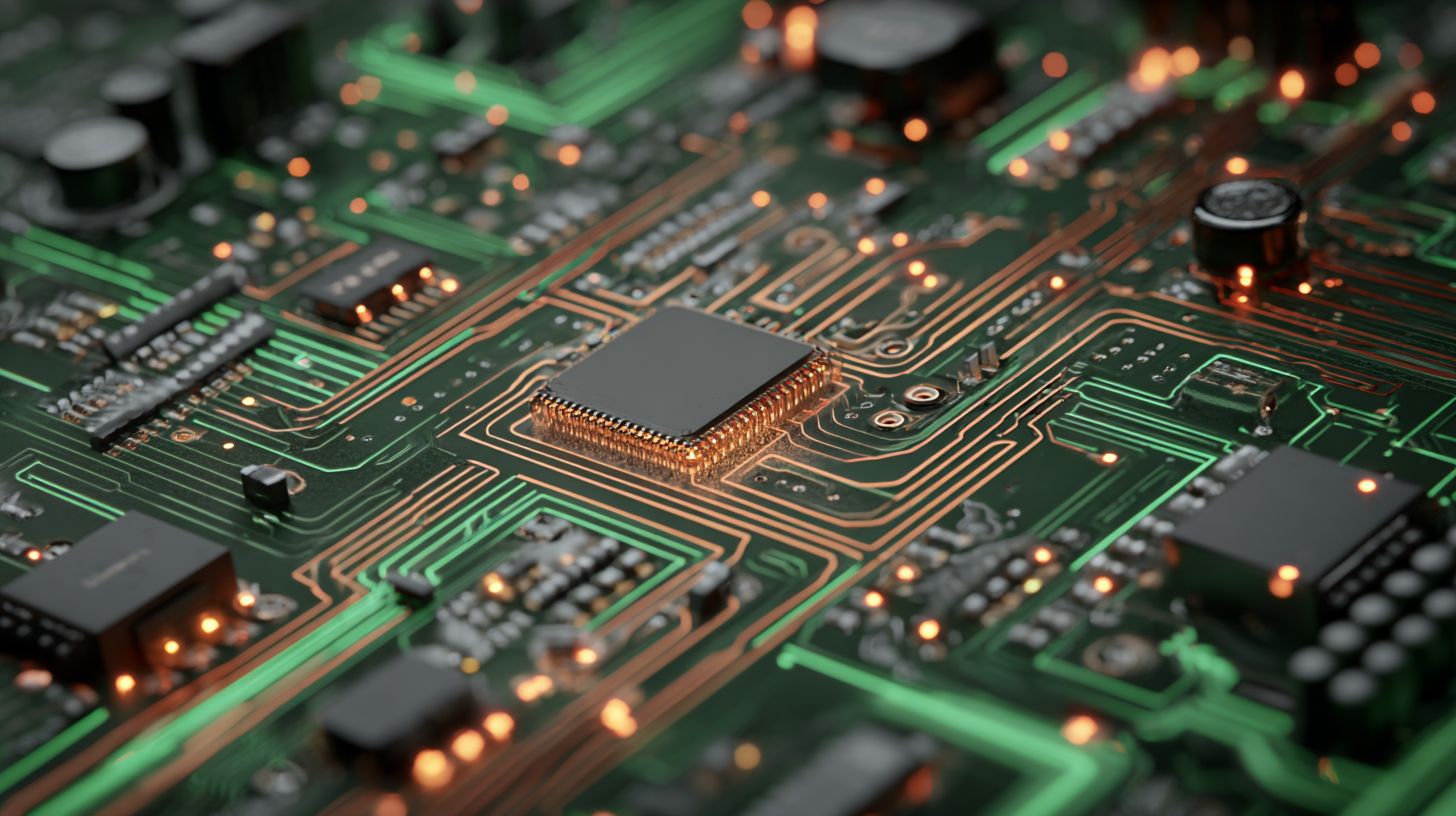
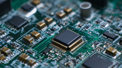
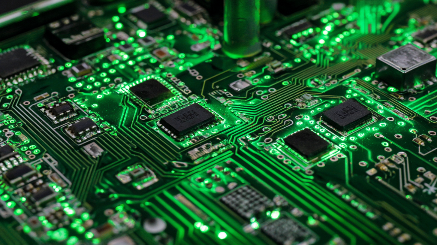
Understanding the basics of PCB design is crucial for both beginners and seasoned professionals in the electronics industry. As of 2023, the global PCB market is projected to reach approximately $80 billion by 2025, driven by the increasing demand for consumer electronics and automotive applications. A solid foundation in essential PCB concepts—including schematic capture, layout design, and signal integrity—can significantly enhance one's ability to create efficient and reliable electronic circuits. According to a recent report from IPC, nearly 70% of PCB design errors stem from inadequate understanding of these fundamental principles, highlighting the importance of mastering the basics.
For beginners, delving into the core concepts is essential. Learning about the differences between various types of PCBs, such as single-sided, double-sided, and multilayer boards, allows designers to make informed choices based on specific project requirements. Furthermore, understanding design tools like computer-aided design (CAD) software is imperative, as they facilitate the visualization and modification of PCB layouts. For professionals, staying updated with evolving industry standards, such as IPC-A-600 for PCB acceptance criteria, is vital in ensuring compliance and maintaining quality. Investing time in mastering these fundamental aspects will undoubtedly enhance design capabilities and promote innovation in the ever-evolving electronics landscape.
Exploring Digital PCB Types: Key Differences and Applications
The shift towards miniaturization in printed circuit board (PCB) design is a pivotal trend that enhances efficiency and reliability across various industries. Digital PCBs are at the forefront of this evolution, offering distinct advantages in size reduction and performance. Unlike traditional analog boards, digital PCBs utilize integrated circuits and can support higher frequencies, making them ideal for applications in telecommunications, consumer electronics, and automotive sectors. As industries strive for more compact and powerful devices, understanding the key differences between digital PCB types becomes essential for both beginners and professionals.
Another significant advancement in PCB technology is the exploration of biodegradable substrates for rigid and flexible circuit boards. These materials present an exciting opportunity to address sustainability challenges in the electronics industry. By employing biodegradable materials, manufacturers can produce circuit boards that minimize environmental impact without compromising performance. The integration of such materials in both rigid and flexible designs reflects a growing trend towards eco-friendly solutions, which is crucial as the industry seeks to balance innovation with ecological responsibility. This transformation highlights the need for designers to adapt and innovate continuously to meet evolving environmental standards and consumer demands.
Understanding PCB Design Techniques: Comparison of Digital PCB Types
Advanced Techniques in PCB Layout: Best Practices for Optimization
As the manufacturing industry undergoes a significant transformation towards smart industrialization,
PCB design techniques are evolving to meet the demands of a more complex,
multi-variety production environment. In this context, optimizing PCB layout
has become crucial. Employing best practices such as
hierarchical design and effective layer stacking can significantly
impact performance and manufacturability. According to a recent industry report, implementing advanced layout
strategies can improve production efficiency by up to 30%, allowing designers to manage resources
more effectively in an era of small-batch production.
Moreover, the rise of AI-driven tools in chip design is reshaping the landscape.
Innovations in automated tools are facilitating the rapid creation of complex circuit layouts, significantly reducing
design time. A notable advancement comes from research indicating that AI can streamline the design process,
achieving results in as little as six hours. This level of efficiency is essential
as the semiconductor market becomes increasingly competitive, demanding not only speed but also precision
in PCB design. As we move toward a future where chiplets and advanced packaging
become the norm, understanding these optimization techniques will be vital for
both beginners and professionals in the field.
Common Pitfalls in PCB Design: Avoiding Mistakes for Success
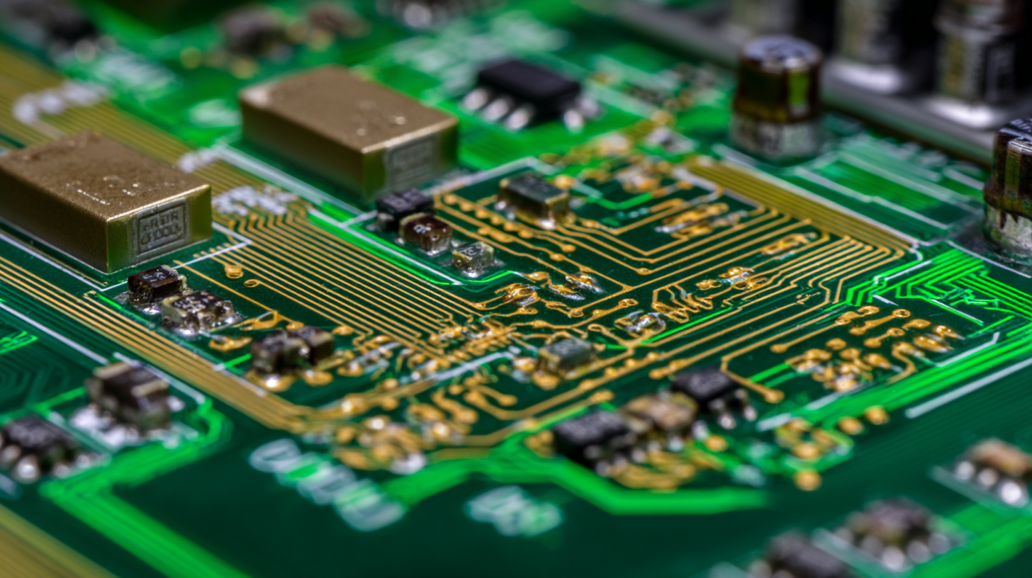
PCB design is an intricate process that often traps both beginners and seasoned professionals in common pitfalls. A recent report by the IPC (Institute for Printed Circuits) highlights that nearly 30% of all PCB projects face significant delays due to design errors. One frequent mistake is overlooking the importance of proper grounding and power distribution. This oversight can lead to electromagnetic interference (EMI) and performance issues. By employing best practices like grounding planes and star connections, designers can significantly mitigate these risks.
Another common error is neglecting the thermal management of PCBs. According to a survey conducted by Mouser Electronics, approximately 40% of PCB failures are linked to inadequate thermal considerations. As component densities increase in modern designs, effective heat dissipation techniques, such as thermal vias and proper component spacing, become crucial. Addressing these issues early in the design phase can save time and resources while enhancing the reliability of the final product. Understanding these common pitfalls and actively avoiding them can lead to successful PCB designs that meet industry standards and customer expectations.
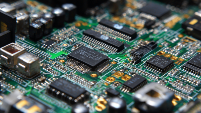
Leveraging Software Tools for Efficient PCB Design Workflow
In the realm of PCB design, leveraging advanced software tools can significantly enhance efficiency and streamline workflows for both beginners and professionals. Recent developments in Electronic Design Automation (EDA) highlight the importance of integrating cutting-edge applications, which can automate complex design processes, allowing engineers to focus on innovation rather than manual tasks. With new AI functionalities added to EDA tools, designers can now experience a considerable boost in productivity and reduction in time-to-market.
**Tips:** When choosing PCB design software, consider platforms that offer cloud-based solutions. These cloud tools not only facilitate real-time collaboration across multidisciplinary teams but also allow for seamless integration with other engineering applications. Additionally, look for software that incorporates AI capabilities to assist with design optimization and error detection, ensuring a smoother design process.
As tools evolve, staying updated on the latest advancements is critical. Regularly exploring new features and updates from leading EDA providers can uncover opportunities to enhance your workflow significantly. Engaging with community forums or webinars can also provide valuable insights and best practices shared by experienced professionals in the field.