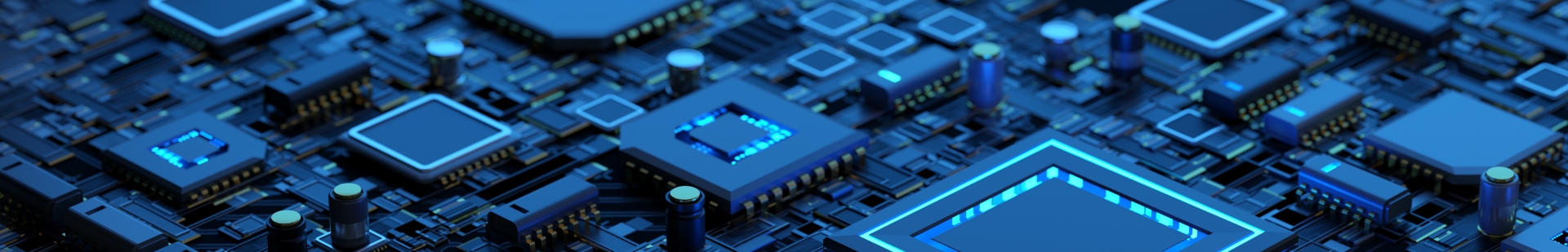
Top PCB Components Trends to Watch in 2025 for Electronics Innovation
As we approach 2025, the landscape for PCB components is poised for revolutionary changes driven by advancements in technology and increasing demands for efficiency and compactness in electronic devices. According to a report by the IPC—Association Connecting Electronics Industries, the global PCB market is expected to reach USD 92 billion by 2025, underscoring the critical role of PCB components in the ongoing innovation within the electronics sector. This growth is propelled by the rising adoption of IoT devices, electric vehicles, and wearables, which all rely heavily on sophisticated and reliable PCB components.
Renowned industry expert Dr. Emily Tran, a leading authority in electronic design and materials science, points out, “The future evolution of PCB components will not only focus on miniaturization but also on enhancing functionality while maintaining sustainability.” Her insights highlight the pressing need for manufacturers to innovate their PCB component designs to meet the challenges posed by both environmental considerations and consumer expectations. The trends we will explore in this article reflect the dynamic and rapidly evolving nature of the PCB components market, shining a light on the innovations that are set to redefine the electronics landscape in the coming years.
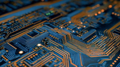
Emerging Materials in PCB Design for Enhanced Performance
In the evolving landscape of PCB design, emerging materials are set to play a pivotal role in enhancing performance and fostering innovation. As the demand for more efficient, durable, and compact electronic devices grows, designers are increasingly turning to advanced materials that offer superior thermal management, signal integrity, and miniaturization capabilities.
Notably, materials such as high-frequency laminates and advanced composite substrates are gaining traction for their ability to maintain performance at higher frequencies and temperatures, which is crucial for 5G and next-generation communication technologies.
Another trend in the development of PCB materials is the move towards eco-friendly options. The industry is witnessing a shift to sustainable materials that not only reduce environmental impact but also meet strict regulatory standards. Biodegradable polymers and recycled substrates are becoming more common, demonstrating that it is possible to combine performance with environmental responsibility.
This alignment of technology and sustainability is influencing the design processes, encouraging manufacturers to rethink traditional material choices and embrace innovation that benefits both their products and the planet. As we look ahead to 2025, these material advancements are expected to significantly shape the future of electronics, driving trends that prioritize efficiency, sustainability, and enhanced performance in PCB design.
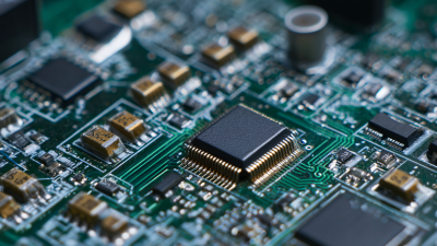
Miniaturization Trends Driving PCB Component Innovations
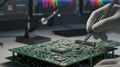
The miniaturization of electronic components is redefining the landscape of PCB design and innovation. As consumer demand for more compact and functional devices grows, manufacturers are compelled to adopt new technologies and materials that allow for smaller, yet more efficient PCB components. This trend is largely driven by advancements in fabrication techniques, enabling the integration of intricate circuits in reduced spaces without compromising performance. Innovations such as ultrathin substrates, sophisticated multilayer designs, and advanced soldering materials are paving the way for the development of next-generation electronics.
In addition to enhancing compactness, miniaturization trends are also fostering greater integration of functionality within PCBs. As components shrink, the potential for more complex systems within a single board increases, leading to lighter, more efficient devices that can perform multiple tasks. This convergence of functionalities not only improves the user experience but also propels the evolution of smart devices, wearables, and Internet of Things (IoT) applications. The synergy between miniaturization and PCB design is thus critical in driving the future of electronic innovation, setting the stage for more versatile and powerful devices in the years to come.
Top PCB Components Trends to Watch in 2025 for Electronics Innovation
| Trend |
Description |
Impact on PCB Design |
Projected Adoption Rate (%) |
| Miniaturization |
Reduction in the size of components to enable smaller PCB designs. |
Increased density and complexity of PCB layouts. |
85% |
| Flexible PCBs |
Use of flexible substrates for applications requiring bending and folding. |
New design approaches for accommodating flexibility in layouts. |
70% |
| Embedded Components |
Integration of components directly into the PCB layers to save space. |
Significant changes in PCB manufacturing processes. |
60% |
| High-Frequency PCBs |
Development of materials to support higher frequency signals efficiently. |
Enhanced signal integrity in high-speed applications. |
50% |
| Sustainable PCB Materials |
Use of environmentally friendly materials in PCB production. |
Shift towards eco-friendly design practices. |
65% |
Integration of Smart Technologies in PCB Components
The integration of smart technologies in PCB components is poised to revolutionize the electronics landscape by 2025. As devices become increasingly connected, the demand for PCBs that can support advanced functionalities like IoT, AI, and machine learning is skyrocketing. Smart PCBs will not only facilitate seamless communication between devices but will also enhance their efficiency, making them capable of processing data in real-time. This transformation allows manufacturers to create smaller, more powerful devices that cater to the needs of modern consumers, paving the way for greater innovation in various industries.
When designing PCBs for smart applications, it's essential to stay updated with the latest trends. One key tip is to prioritize modular designs that allow for easy upgrades and integration of new technologies. This flexibility can significantly extend the lifespan of electronic devices and reduce waste. Additionally, using advanced materials that support high-frequency signals and thermal performance will ensure reliability and longevity in smart devices.
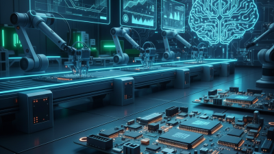
Investing in automation and smart manufacturing processes is another crucial consideration. By leveraging AI and robotics in PCB production, manufacturers can achieve higher precision and efficiency, minimizing human error while lowering production costs. Embracing these smart technologies in PCB components not only promotes innovation but also fosters sustainability through optimized resource use and reduced environmental impact.
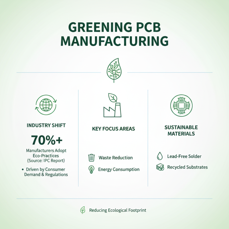
Sustainability Practices in PCB Manufacturing and Component Sourcing
Sustainability is becoming a cornerstone in the PCB manufacturing industry as companies pivot towards more environmentally friendly practices. According to a recent report by IPC (Institute of Printed Circuits), more than 70% of electronics manufacturers are implementing sustainability initiatives, with a significant focus on reducing waste and energy consumption. This trend is largely driven by growing consumer demand for eco-friendly products and regulatory pressure to adhere to stricter environmental standards. As such, PCB manufacturers are increasingly adopting greener materials, such as lead-free solder and recycled substrates, which contribute to minimizing the ecological footprint of electronic devices.
Additionally, the sourcing of PCB components is undergoing a transformative shift towards sustainability. The Global Electronics Council reports that over 60% of electronic components are now being sourced from suppliers with verified sustainability practices. This emphasis on responsible sourcing not only aligns with the growing corporate social responsibility (CSR) goals of manufacturers but also enhances the overall supply chain resilience. Implementing sustainable sourcing strategies not only reduces environmental impact but also fosters innovation by encouraging the development of new materials and technologies that further drive the industry towards a circular economy. As we move towards 2025, these sustainable practices in PCB manufacturing and component sourcing will undoubtedly shape the future of electronics innovation.
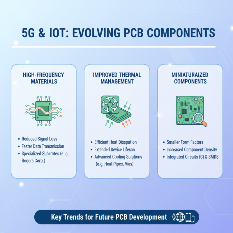
Impact of 5G and IoT on PCB Component Development Trends
The advent of 5G and the Internet of Things (IoT) is significantly shaping the landscape of PCB component development. As devices become more interconnected and demand for higher data speeds increases, PCB manufacturers are focusing on innovations that cater to these advancements. High-frequency materials, improved thermal management solutions, and miniaturized components are emerging as crucial trends. These advancements allow for greater efficiency and performance in devices ranging from smartphones to smart home appliances.
Tips: When designing for 5G and IoT applications, consider utilizing advanced simulation tools during the prototyping phase. This helps identify potential issues related to signal integrity and thermal performance early in the design process, allowing for timely adjustments and improvements.
Additionally, the integration of sensors within PCBs is becoming increasingly popular. This enables devices to monitor their environment and communicate data more effectively. With the move toward more intelligent devices, engineers should prioritize flexibility in PCB layout to accommodate future upgrades and functionality enhancements.
Tips: Always keep an eye on component encapsulation and shielding when designing for applications with high electromagnetic interference. Ensuring robust designs will mitigate potential performance drawbacks in densely populated electronic circuits.