Top PCB Design Tips: Maximize Efficiency and Reduce Errors Fast
In the world of electronics, efficient and error-free PCB design is crucial for successful product development. Renowned PCB design expert Dr. Jane Smith emphasizes, "A well-structured PCB layout not only improves performance but also minimizes the potential for costly revisions later in the production cycle." This aphorism captures the essence of why adhering to best practices in PCB design is imperative for engineers and designers alike.
As technology advances and market demands escalate, the urgency for optimizing PCB design processes has never been greater. With the increasing complexity of electronic devices, incorporating the latest techniques and methodologies can significantly streamline workflows while enhancing the reliability of the final product. By focusing on key considerations such as component placement, signal integrity, and thermal management, designers can navigate common pitfalls that lead to errors and inefficiencies.
Ultimately, maximizing efficiency and reducing errors in PCB design is not just about improving the design process; it is about fostering innovation and ensuring that electronic products meet the high standards of reliability and performance expected in today’s competitive landscape. Embracing strategic design tips can empower engineers to create cutting-edge solutions that resonate in the market.
Understanding PCB Design Basics for Enhanced Efficiency
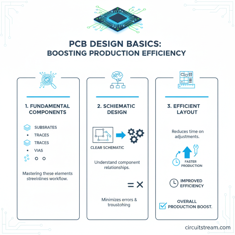
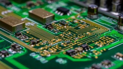
Understanding the basics of PCB design is crucial for enhancing overall efficiency in the production process. A well-structured approach begins with familiarizing oneself with the fundamental components of printed circuit boards, such as substrates, traces, and vias. By mastering these elements, designers can streamline their workflow, reducing the time spent on troubleshooting and adjustments. Starting with a clear schematic ensures that each component's relationship is understood before moving to the layout phase, minimizing errors that could arise from misinterpretation.
Additionally, incorporating design software that offers real-time error checking can significantly boost efficiency. Many modern PCB design tools include features like design rule checks (DRC) and component footprint libraries, which help avoid common pitfalls. By utilizing these resources, designers can achieve a more accurate layout, promoting better signal integrity and reducing the likelihood of revisits in the prototyping stage. Ultimately, a solid understanding of PCB design fundamentals paired with advanced tools can lead to more efficient processes and higher-quality end products.
Key Software Tools for Streamlined PCB Design Processes
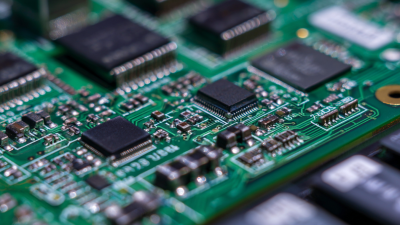
When it comes to PCB design, the right software tools can make a significant difference in enhancing efficiency and reducing errors. Leveraging advanced CAD software is essential; tools like Altium Designer and Eagle not only streamline the design process but also facilitate the creation of complex layouts with precision. These programs offer features such as real-time design rule checking and automated routing, which minimize the chances of human error and save valuable time.
In addition to traditional CAD applications, simulation tools like SPICE and Ansys Electronics Desktop provide engineers with the ability to validate designs before physical prototyping. By simulating circuit behavior under various conditions, designers can identify and correct potential issues early in the process. Incorporating version control systems and collaboration platforms ensures that team members can work together efficiently, share ideas, and maintain the integrity of the design workflow. Emphasizing these software tools can greatly enhance the PCB design process, leading to quicker turnarounds and more reliable final products.
Best Practices for Component Placement and Schematic Layout
Effective component placement and schematic layout are crucial for efficient PCB design. Proper component placement begins with understanding the circuit's functionality and flow. Grouping related components together minimizes the length of connections, reducing parasitic capacitance and inductance. Additionally, maintaining a consistent orientation for polarized components can streamline the assembly process, saving time and reducing the likelihood of errors during both fabrication and troubleshooting.
When it comes to schematic layout, clarity is paramount. Using clear labels and logical connections helps to prevent confusion during the design review process. Employing standardized symbols and adhering to design rules not only enhances readability but also ensures that the schematic can be easily interpreted by other engineers. It's also beneficial to utilize hierarchical designs for complex systems, breaking down the circuit into manageable sections that can be understood independently, further minimizing the potential for mistakes during later stages of the design.
Effective Techniques for Error Detection and Correction
Effective error detection and correction is crucial in PCB design to ensure functionality and reliability. One of the key techniques is implementing design rule checks (DRC) within your PCB design software. DRC helps in identifying violations of specified rules, such as trace width or spacing, before the board goes into manufacturing. Regularly running DRC will catch potential issues early, reducing costly revisions later.
Another efficient method is using simulation tools to test your design before production. Simulations allow you to visualize how the PCB will behave under various conditions, giving you the opportunity to spot and correct errors that may arise during operation. This proactive approach not only saves time but also enhances the design's overall performance.
Lastly, peer reviews play a significant role in error detection. Having another set of eyes review your design can uncover mistakes that you might overlook. Encourage team collaboration by utilizing tools that allow for easy sharing and annotation of designs. This can create a culture of quality where errors are minimized through collective effort. Incorporating these techniques will significantly contribute to maximizing efficiency and reducing errors in PCB design.
Top PCB Design Tips: Maximize Efficiency and Reduce Errors Fast - Effective Techniques for Error Detection and Correction
| Technique |
Description |
Efficiency Gains |
Error Reduction Rate |
| Design Rule Check (DRC) |
Automatically verify that the design complies with all manufacturing requirements. |
20% Increase |
30% Reduction |
| Signal Integrity Analysis |
Analyze the PCB design for potential signal integrity issues that could affect performance. |
15% Increase |
25% Reduction |
| Layer Management |
Optimize layer usage to minimize complexity and improve routing efficiency. |
10% Increase |
20% Reduction |
| Automated Routing Tools |
Utilize software tools to assist in PCB routing to enhance layout performance. |
25% Increase |
40% Reduction |
| Prototype Testing |
Conduct physical testing on prototypes to identify any design flaws before mass production. |
30% Increase |
50% Reduction |
Tips for Optimizing PCB Fabrication and Assembly Efficiency
Optimizing PCB fabrication and assembly efficiency is crucial for reducing costs and improving the speed of production. One effective approach is to simplify the design by minimizing the number of layers and components. This not only streamlines the manufacturing process but also helps in avoiding potential errors that could arise from more complex designs. Utilizing a modular design approach can further enhance efficiency, allowing for easier assembly and maintenance.
Another tip is to engage in proactive communication with manufacturers. Sharing design files early in the process and requesting feedback can help identify potential issues before production begins. This collaboration can lead to modifications that enhance manufacturability and yield higher quality products. Additionally, implementing design rule checks (DRCs) within PCB design software can catch errors early, saving time and resources during the manufacturing phase. By prioritizing these strategies, designers can ensure a smoother workflow and more reliable outcomes in PCB fabrication and assembly.