What is a Printed Circuit Board and How Does It Work?
In the world of electronics, the printed circuit board (PCB) stands as a cornerstone of innovation. Dr. Emily Chen, a renowned expert in PCB design, once stated, "The printed circuit board is where ideas come to life." This encapsulates the essence of how PCBs connect and power modern electronic devices.
Printed circuit boards serve as the backbone of smartphones, computers, and countless gadgets. They enable intricate connections between various electronic components. Understanding how a PCB functions can seem daunting, yet it is crucial for anyone interested in electronics. The layout, materials, and design all play pivotal roles in performance.
However, the process of creating an efficient printed circuit board is not without challenges. Designers often face difficulties in achieving the perfect balance between size and functionality. Each decision can lead to significant impacts on a product's overall success. Exploring these aspects can lead to better designs and innovations for the future.
What is a Printed Circuit Board (PCB)?
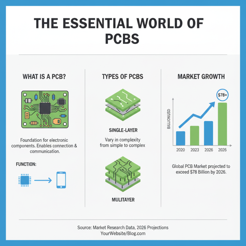
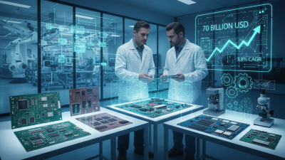
A Printed Circuit Board (PCB) is essential in modern electronics. It provides the foundation for electronic components to connect and communicate. PCBs can vary in complexity, from simple single-layer boards to intricate multilayer configurations. Data from market research indicates the global PCB market is projected to reach over $78 billion by 2026, reflecting the increasing demand for electronics.
The materials used in PCBs matter. Common substrates include fiberglass and various polymers. These materials enable durability and electrical insulation. However, the production process can be inefficient, leading to waste. It's estimated that around 30% of materials can be lost during manufacturing. Designers must balance quality with cost-effectiveness.
**Tip:** When selecting PCB materials, consider both performance and environmental impact. Newer techniques can help reduce waste.
Another challenge is design complexity. As devices become smaller, PCB designs require precision. The number of layers and components can increase the risk of errors. A reported 20% of prototypes face issues during testing that delay production. Improvements must focus on design verification processes.
**Tip:** Use simulation tools during the design phase to catch errors early. This can save time and resources.
The Structure and Components of a PCB
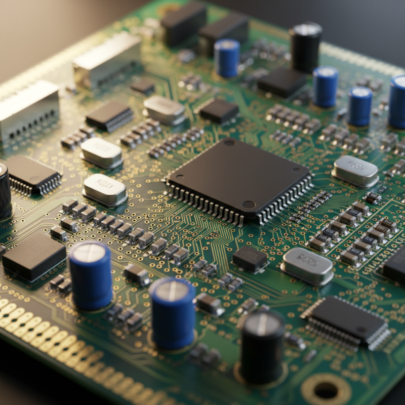
Printed Circuit Boards (PCBs) are essential in modern electronics. They serve as a foundation for connecting various electronic components. The structure of a PCB typically includes layers of conductive pathways, insulation, and sometimes additional materials for support. Common materials used are fiberglass and epoxy.
A typical PCB consists of several key components. Conductive traces, usually made of copper, connect different parts. Pads are areas where components like resistors and capacitors are soldered. Additionally, vias allow electrical connections between layers. According to industry reports, the global PCB market was valued at approximately $60 billion in 2022. This figure highlights the importance of PCBs in the tech industry.
Challenges exist in PCB design and manufacturing. Complexity can lead to errors, especially in multi-layer boards. Designers need to ensure that components fit well. Poor layout can cause signal interference. As technology advances, there’s a push for smaller, more efficient designs. This necessitates ongoing research and development in the field. Industry experts predict a steady growth in demand, hinting at an ever-evolving landscape.
How PCBs are Fabricated and Manufactured
The fabrication of printed circuit boards (PCBs) begins with the selection of materials. Copper is commonly used for the conductive layers. The substrate is often made of fiberglass. This combination provides durability and electrical performance.
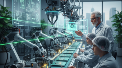
Once materials are chosen, the design is created using specialized software. This involves laying out the circuit, including pads and traces. The design is then printed onto a film, which acts as a guide for etching. Photolithography can be used to transfer the design onto the copper layer. Essential steps are often overlooked, leading to errors in final products.
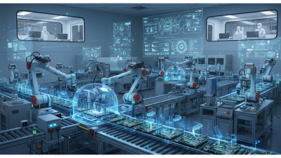
Next, the actual manufacturing process begins. PCBs are drilled to create holes for components. Etching removes excess copper, shaping the circuit. However, inconsistencies can arise during this process. Issues may include inadequate etching, leading to weak connections. Small mistakes can result in significant problems later. Identifying such flaws early can save time and resources. The final steps include solder mask application and printing labels, preparing the PCB for assembly.
What is a Printed Circuit Board and How Does It Work?
| Dimension |
Description |
| Definition |
A printed circuit board (PCB) is a board used in electronics to connect components using conductive pathways. |
| Materials |
Typically made from fiberglass, epoxy, or other laminate materials for insulation. |
| Layers |
Can have multiple layers to accommodate complex circuitry and density. |
| Fabrication Process |
Involves design, printing, etching, and layering processes to create the final board. |
| Common Applications |
Used in computers, mobile phones, appliances, and various electronic devices. |
| Functionality |
Allows for electrical connections and signal transmission between components. |
| Testing |
PCBs undergo rigorous testing for integrity and performance before deployment. |
The Functionality of a PCB in Electronic Devices
A printed circuit board (PCB) serves as the backbone of electronic devices. It connects various components, ensuring they communicate effectively. These boards are made from non-conductive materials, like fiberglass. The circuitry is printed on their surfaces. Components are then soldered onto the PCB, allowing them to function together.
The PCB's design impacts the performance of electronic devices. A poorly designed PCB can lead to signal interference and circuit failures. For example, if traces are too close, unwanted crosstalk may occur. Similarly, inadequate spacing can cause overheating. These issues highlight the importance of careful planning in circuit design.
Moreover, PCBs are critical in managing power distribution. They help regulate voltage, ensuring each component receives the energy it needs. Without this regulation, devices could malfunction or even become damaged. A well-functioning PCB is essential for the reliability of modern electronics.
Common Types of PCBs and Their Applications
Printed Circuit Boards (PCBs) come in various types. Each type serves unique applications across industries. The most common types include single-sided, double-sided, and multilayer PCBs. Single-sided PCBs, with components on one side, are easy to design. They are commonly used in simple electronics like calculators.
Double-sided PCBs allow for more complexity. Components can be placed on both sides, enabling denser circuit designs. This is ideal for devices like audio equipment and industrial machinery. According to a 2022 market report by IPC, demand for double-sided PCBs has increased by 15% in two years. Multilayer PCBs offer even more complexity. They integrate several layers of circuits, suitable for smartphones and aerospace applications. With growing technologies, multilayer PCBs are expected to dominate the market, reaching a valuation exceeding $27 billion by 2025.
While these PCBs offer great advantages, they come with challenges. Complexity can lead to higher production costs. Manufacturing defects can also be harder to diagnose in multilayer boards. Industry professionals note that maintaining quality control is crucial. Even minor errors can result in significant failures in high-stakes applications. The evolving landscape highlights the need for constant innovation. Understanding these types and their limitations is essential for designing reliable electronic systems.