2026 Best PCB Design Trends You Need to Know?
In the rapidly evolving world of PCB design, staying ahead of trends is crucial. The global PCB market is projected to reach $93.8 billion by 2026, significantly impacting various industries. A recent study by ResearchAndMarkets highlights the increasing complexity and demand for innovative design solutions. Experts emphasize the importance of adapting to these changes. As noted by Dr. Sarah Chen, a leading authority in PCB design, “Understanding emerging trends can propel businesses to new levels of success.”
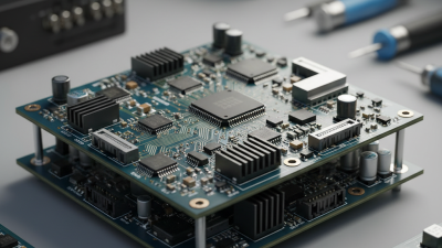
The rise of miniaturization and IoT has transformed PCB design dynamics. Today’s designs must accommodate smaller components while ensuring high performance. The growing trend of flexible and wearable technology also challenges traditional design approaches. It’s not just about aesthetics; engineers must grapple with functional reliability and manufacturing feasibility. The integration of AI in PCB design is on the rise, yet it raises questions about efficiency and management of resources in a fast-paced market.
As we approach 2026, companies must reflect on their design methodologies. Embracing new software tools can enhance productivity. However, the adaptation process is not without its challenges. The PCB design landscape is both an opportunity and a hurdle. Keeping pace with innovation demands thoughtful consideration and ongoing education within the field. The future of PCB design is bright, but it requires commitment to change.
Emerging Materials in PCB Design for Enhanced Performance
Emerging materials are crucial in PCB design. They drive performance and reliability. Recent studies show that new materials can improve thermal management, electrical conductivity, and durability. For example, using polyimide substrates can enhance heat resistance, allowing designs to operate at higher temperatures. This is vital for advanced applications like automotive electronics.
Another promising material is copper-clad laminates. These laminates reduce signal loss significantly. Data from industry reports indicate that signal integrity improves by 20% when using high-performance laminates. This increase leads to better communication speeds and efficiency in devices. Furthermore, the use of alternative conductive materials, like graphene, is emerging. Graphene offers superior electrical properties but remains costly and challenging to integrate.
However, the transition to these materials isn’t without challenges. Manufacturers face high costs and a steep learning curve. There's concern about compatibility with existing manufacturing processes. Also, the long-term reliability of some new materials is not fully understood. Balancing performance with production capabilities remains a complex issue. As the industry evolves, questions linger about sustainable sourcing and how manufacturers will address these hurdles.
Miniaturization Trends in PCB Designs for Compact Electronics
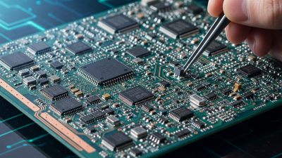
The miniaturization of PCB designs is a pivotal trend shaping compact electronics. As consumer demand rises for smaller devices, manufacturers must adapt. A recent industry report indicates that the global PCB market is projected to reach $85 billion by 2026. This growth is fueled by the increasing demand for miniaturized electronics across sectors like automotive, healthcare, and telecommunications.
Engineers face challenges in maintaining functionality while reducing size. For example, achieving high-density interconnections requires precision and advanced manufacturing techniques. Some designs prioritize multilayer configurations to save space, yet this often complicates the assembly process. As a result, engineers are exploring alternatives such as embedded components and flexible PCB solutions. These efforts can yield significant lead time reductions, but they also introduce new complexities.
However, the push for miniaturization isn't without drawbacks. Smaller PCBs can lead to overheating issues due to lack of space for proper heat dissipation. According to recent studies, about 30% of electronic failures result from thermal stress. Thus, designers must balance size and reliability, which is no small feat. As we continue down this path, the challenge will be to innovate without sacrificing the performance that end users expect.
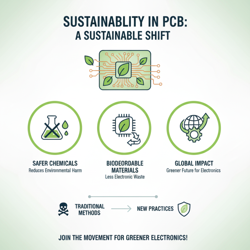
Sustainability Practices in PCB Manufacturing and Design
Sustainability is becoming crucial in PCB manufacturing and design. Companies are seeking eco-friendly materials and practices. Traditional methods often involve harmful chemicals, which can damage the environment. Switching to safer alternatives is essential. Biodegradable materials are gaining attention. They reduce electronic waste significantly.
Another trend is energy-efficient manufacturing. Reducing energy consumption lowers costs and carbon footprints. However, many factories still rely on outdated practices. This raises concerns about their commitment to sustainability. Implementing renewable energy sources, like solar or wind, is a vital step. Yet, some manufacturers resist change due to initial costs.
Recycling old PCBs is also a challenge. Only a small percentage of electronic waste is recycled. Encouraging designs that facilitate easy disassembly is important. Many designers overlook this, focusing instead on aesthetic appeal. The industry must shift priorities. By embracing sustainability, we can create a healthier planet, one PCB at a time.
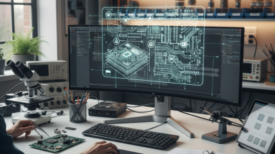
Advancements in PCB Design Software and Simulation Tools
In 2026, advancements in PCB design software are reshaping how engineers approach their projects. These tools now offer enhanced simulation capabilities. Designers can visualize circuit behavior before actual production. This saves time and reduces waste. However, not all software solutions offer the same level of reliability. Some may have bugs that can lead to incorrect assumptions.
Moreover, simulation tools are evolving. They allow for real-time feedback during the design phase. This enables quicker iterations and adjustments. Engineers can explore various configurations effortlessly. Yet, the learning curve can be steep. New users often struggle with complex interfaces. This can hinder productivity at critical times. Adapting to these tools requires patience and practice.
The integration of AI into design software adds another layer of complexity. AI can assist in optimizing layouts and identifying potential issues. Still, it is not infallible. AI-generated designs may overlook specific unique requirements. It is essential to balance automation with human insight. Ultimately, blending technology with traditional design methods could yield the best results.
Integration of IoT and Smart Technologies in PCB Layouts
The integration of IoT and smart technologies in PCB layouts is transforming the electronics landscape. Modern designs must accommodate multiple functionalities. This integration demands careful planning and innovative strategies. Engineers need to prioritize connectivity and efficiency, ensuring the devices can communicate effectively.
Incorporating IoT features often requires advanced materials and specific components. The choice of materials impacts both performance and cost. Not all designs achieve the desired balance between functionality and manufacturability. Prototyping and testing can reveal unexpected challenges. Paying attention to thermal management is essential as devices become smarter and more compact.
Additionally, sustainability is a growing concern. Designers must consider eco-friendly options. It’s a challenge to stay within budget while also being environmentally responsible. Many engineers are still learning how to seamlessly integrate these elements. As technology evolves, so should the approaches to PCB design.