2026 Top PCB Manufacturing and Assembly Companies?

A shortlist of the 2026 top PCB manufacturing and assembly companies should begin with evidence, not slogans. The market is changing as electronics become more compact, connected, and power-hungry. The World Semiconductor Trade Statistics (WSTS) organization reported global semiconductor sales of $627.6 billion in 2024, up 19.1% from 2023. That figure is not a PCB market estimate, but it signals the scale of demand behind many circuit-board programs.

Demand alone does not identify a reliable supplier. Buyers should compare each company’s board capabilities, assembly services, production locations, engineering support, and ability to meet delivery schedules. Ask about multilayer and high-density interconnect (HDI) experience, prototype handling, inspection methods, and traceability. Details matter. IPC standards offer useful reference points: IPC-6012 covers qualification and performance requirements for rigid printed boards, while IPC-A-610 sets acceptance criteria for electronic assemblies. They help frame discussions, but certification or compliance claims still need verification.

This guide will assess providers through practical criteria, including technical fit, quality controls, scalability, and customer support. A large factory may suit a high-volume program, while a responsive regional partner may better serve rapid prototypes. Neither is automatically the better choice. Supplier websites can make every capability sound routine; real projects often expose gaps in documentation, communication, or process control. Those details deserve a closer look. The goal is not to declare one universal winner, but to help engineering and procurement teams build a shortlist suited to their products, volumes, and risk tolerance.

2026 Top PCB Manufacturing and Assembly Companies?

Understanding PCB Manufacturing and Assembly in 2026

In 2026, PCB manufacturing and assembly begin with decisions made long before a board reaches the factory. Layer count, copper thickness, material choice, and trace spacing affect performance and cost. For high-speed designs, engineers may specify controlled impedance and review the stack-up with the fabricator. Small changes matter. A connector moved by a few millimeters can alter routing or assembly access.

Fabrication typically involves imaging copper patterns, etching, drilling, plating, and applying solder mask. Each step has limits. A very dense layout may require tighter process control, while unusually thick copper can complicate fine traces. Automated optical inspection can identify visible defects, but it cannot prove every electrical connection works. Test points and electrical testing still matter.

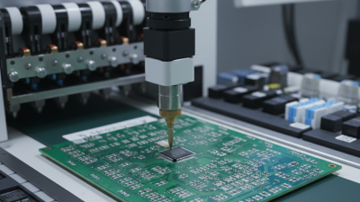
Assembly adds another set of practical checks. Solder paste is deposited through a stencil, components are placed, and the board passes through a reflow oven. Temperature profiles must suit the board and its components. Afterward, visual inspection and automated optical inspection can catch misplaced parts or solder issues; hidden joints may need X-ray review. Yet inspection is not a substitute for clear design files. Even experienced teams sometimes discover that a technically correct board is awkward to assemble, so early design reviews and prototype builds remain useful.
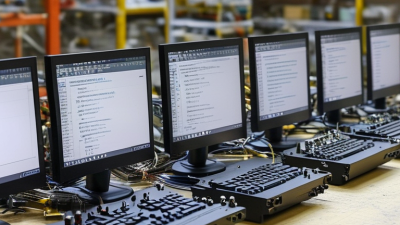

PCB Manufacturing in 2026: Common Copper Foil Weights

Nominal copper thickness is a useful material specification when comparing PCB manufacturing capabilities.

Values use the nominal conversion of 1 oz/ft² of copper to approximately 34.8 μm. Finished copper thickness can differ because of plating and etching; actual specifications depend on the board design and manufacturing process.

How PCB Companies Are Evaluated and Ranked

A credible PCB ranking should measure repeatable production, not polished claims. Reviewers can compare process controls, engineering depth, and documented quality results. For fabrication, useful evidence includes layer-count capability, line-width control, drill accuracy, impedance data, and inspection records. Assembly evaluations should examine component sourcing controls, solder-paste inspection, reflow profiles, and functional-test coverage. Small details matter.

Experience shows that performance depends on fit. A supplier handling simple prototypes may not suit dense boards or stable volume builds. Evaluators should request sample reports, trace materials through each production lot, and compare quoted lead times with delivery records. Defect rates need context: board complexity and reporting methods can change the numbers.

Rankings should also assess communication, engineering support, change control, and corrective-action quality. Ask how a factory responds when a test coupon misses its target or a solder joint fails inspection. A clear root-cause report is more useful than a broad promise. Public data is often incomplete, and rankings can reward visibility over capability. That comparison is imperfect. Treat scores as one input, then check them against the board’s materials, tolerances, and production forecast.

Leading PCB Manufacturing and Assembly Companies

Leading PCB manufacturing and assembly companies do more than etch copper and place components. They connect design review, fabrication, sourcing, assembly, inspection, and delivery. A strong partner can explain how a narrow trace, dense via field, or fine-pitch component affects yield. Ask for sample inspection records and clear process limits, not just a fast quote. Small details matter.

The market is growing, but growth alone does not prove supplier quality. Grand View Research valued the global PCB market at USD 76.2 billion in 2023 and projected a 5.6% compound annual growth rate from 2024 to 2030. WSTS’s November 2024 forecast estimated semiconductor sales would rise 19% in 2024, to about USD 627 billion. That broader electronics demand can increase pressure on board capacity and component sourcing. Buyers should check current lead times and approved alternates.

A useful supplier review includes stack-up capability, trace-width control, solder-joint inspection, and documented electrical testing. Ask how engineering changes are controlled between prototype and production. Request a small pilot run before committing to volume. The first run may be awkward. That is often when unclear drawings, footprint errors, or assembly assumptions become visible. A polished presentation is helpful, but repeatable process records matter more.

Key Services and Technologies Offered by Top Providers

Leading PCB manufacturing and assembly providers combine design review, fabrication, component sourcing, and production testing. Their engineers can check Gerber files, stack-ups, and drill plans before a panel reaches the production line. This early review may catch narrow spacing or an unsuitable via structure. Small corrections matter.

Fabrication services often include multilayer boards, controlled-impedance routing, fine-pitch features, and HDI microvias. Providers may also advise on copper weight, laminate choice, and thermal demands. For assembly, surface-mount technology handles compact components, while through-hole processes support parts that need stronger mechanical anchoring. Some projects use both. It depends.

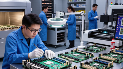
Inspection methods can include automated optical inspection, X-ray checks for hidden solder joints, and electrical continuity testing. Functional testing adds another layer by checking whether an assembled board performs under defined operating conditions. Ask how test limits, defect records, and lot traceability are documented. Clear records help teams investigate failures, though testing cannot remove every risk.

Reliable providers should explain capacity, lead times, and process limits in plain terms. Request sample reports and confirm how engineering changes are controlled. A polished capability list is useful, but not enough; real performance can vary between prototypes and larger production runs. That gap deserves attention.

2026 Top PCB Manufacturing and Assembly Companies? - Key Services and Technologies Offered by Top Providers

Capability Area Common Services Relevant Technologies and Processes Typical Applications Quality and Verification Methods
Rigid PCB fabrication Single-sided, double-sided, and multilayer board fabrication; prototype and production runs. Copper-clad laminates, subtractive copper patterning, plated through-holes, solder mask, and surface finishes such as HASL, ENIG, and OSP. Control boards, consumer electronics, industrial equipment, and computing hardware. Electrical continuity and isolation testing, visual inspection, and dimensional checks.
HDI and advanced multilayer boards High-density interconnect design and fabrication for compact layouts with dense routing. Laser-drilled microvias, sequential lamination, blind and buried vias, and fine-line patterning. Smartphones, compact computing devices, medical electronics, and advanced communications equipment. Microsection analysis, electrical testing, and inspection of via and layer registration.
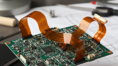
Flexible and rigid-flex circuits Flexible circuit fabrication and rigid-flex board production for assemblies requiring bends or three-dimensional packaging. Polyimide substrates, flexible copper laminates, coverlays, stiffeners, and controlled bend-zone design. Wearables, cameras, medical devices, aerospace electronics, and compact interconnects. Continuity testing, visual inspection, and design checks for bend areas and layer transitions.
Specialty substrate and thermal boards Fabrication of boards designed for thermal management, electrical isolation, or high-frequency performance. Metal-core PCBs, ceramic substrates, and RF laminates selected for the electrical and thermal requirements of the design. LED lighting, power conversion, radio-frequency circuits, and high-power electronics. Electrical testing, material and dimensional checks, and thermal or RF testing when specified.
Surface-mount assembly Component sourcing support, solder-paste printing, component placement, reflow soldering, and assembly of SMT components. Automated pick-and-place equipment, stencil printing, reflow ovens, and lead-free solder processes where specified. Most compact electronic products, including control modules, communications devices, and consumer equipment. Solder-paste inspection, automated optical inspection (AOI), and in-circuit or functional testing as required.
Through-hole and mixed-technology assembly Through-hole component insertion and soldering, combined with surface-mount assembly on the same board. Wave soldering, selective soldering, hand soldering, and mixed-technology process sequencing. Power supplies, connectors, industrial controls, and products using mechanically robust components. Visual inspection, AOI for applicable components, and electrical or functional testing.
Fine-pitch and package assembly Assembly of fine-pitch components and packages with connections beneath the component body. BGA and QFN placement, controlled reflow profiles, and X-ray inspection for joints hidden from direct visual inspection. Computing, networking, telecommunications, and other high-density electronic assemblies. AOI, X-ray inspection, electrical testing, and rework procedures appropriate to the package and assembly.
Engineering and design support Design-for-manufacturing (DFM) feedback, fabrication data review, stack-up planning, and assembly readiness checks. Gerber or other fabrication data review, drill-file checks, bill-of-materials review, and manufacturability analysis. New product introduction, design revisions, and preparation for prototype or volume production. Design-rule review, data validation, and documented approval of manufacturing requirements.
Inspection, testing, and traceability Inspection and test services selected according to product risk, design requirements, and customer specifications. AOI, X-ray inspection, flying-probe or fixture-based electrical testing, and functional test procedures. Products requiring documented inspection, production controls, or verification before shipment. Inspection records, test results, lot identification, and material traceability where offered and specified.
Selection note: Service availability, materials, process limits, certifications, inspection coverage, and production capacity vary by provider and project. Confirm requirements directly with the manufacturer before placing an order.

How to Choose a PCB Partner for Your Project

Choosing a PCB partner means checking how well its process fits your design, not just comparing prices. Share your schematic, board files, layer count, and expected volume. Ask whether engineers review the design for manufacturability before production. A useful review should flag issues such as narrow clearances, awkward panelization, or unclear impedance requirements. Details matter.

Look for clear answers about materials, stack-up control, solder-mask options, and inspection methods. For assembly, ask how components are sourced and how defects are recorded. Request sample inspection reports or yield data from comparable work, with sensitive customer information removed. A small pilot run can reveal problems that a quote cannot: a connector may not align, or a fine-pitch part may need a stencil adjustment. Ask why.

Evaluate communication, too. Can the team explain a delay, identify the affected batch, and provide a realistic revised schedule? Compare lead times against your actual build plan, not an ideal estimate. No partner is flawless, and a polished sales response proves little. I would still want to see how the team handles an imperfect first run, because that is often where its engineering discipline becomes visible.