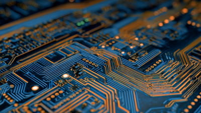
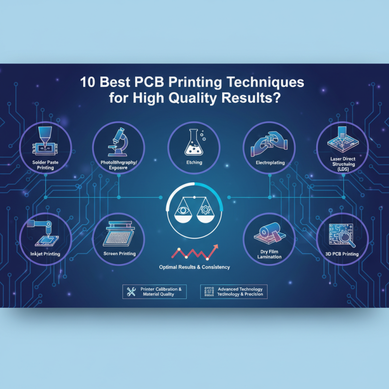
In today's fast-paced electronics industry, high-quality PCBs are crucial. Achieving optimal results in PCB printing requires a deep understanding of various techniques. This article explores ten of the best practices for successful PCB printing. Each technique has its unique strengths and applications.
As technology advances, PCB printing has become more intricate yet accessible. However, many still struggle with consistency. Factors such as material quality and printer calibration play significant roles in the final product. Understanding how these elements interact can lead to better results.
While many methods exist, not all yield the desired outcome. Some may produce aesthetically pleasing boards but lack in functionality. It's essential to reflect on both the visual and performance aspects of PCB printing. The balance between beauty and utility often determines the success of a project.
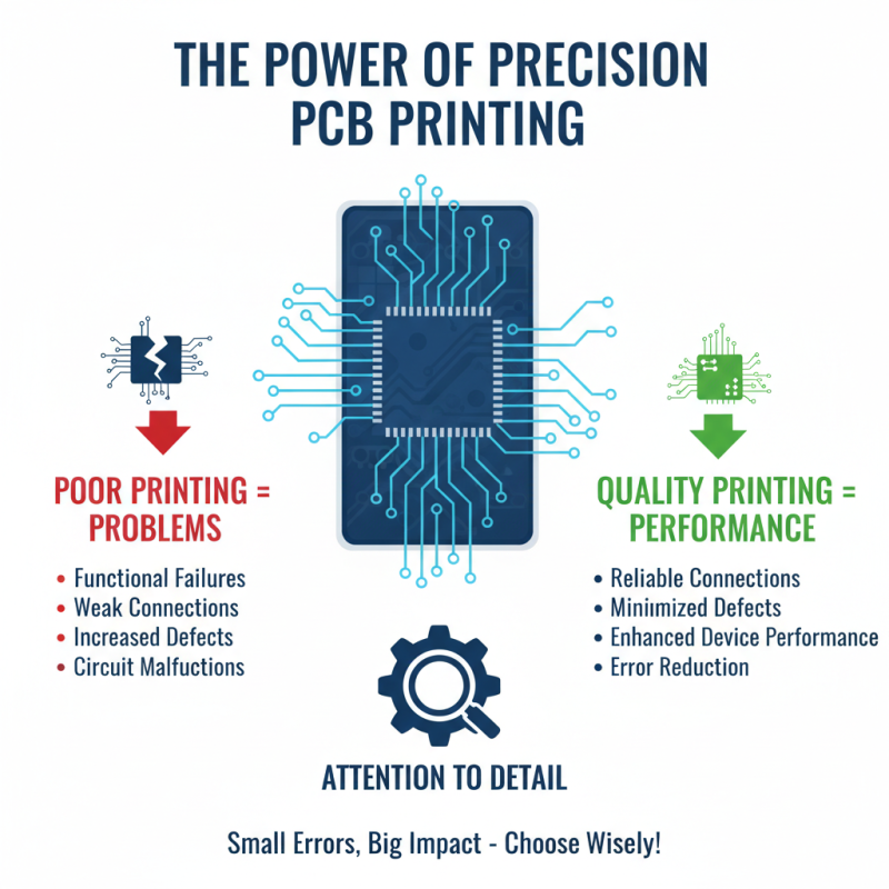
When it comes to PCB printing techniques, quality is paramount. High-quality printed circuit boards (PCBs) are essential for ensuring reliability in electronic devices. One report highlighted that nearly 25% of PCB failures stem from poor printing quality. Selecting the right printing technique can mitigate these issues.
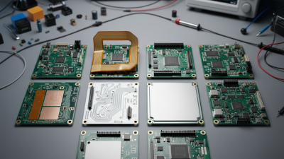
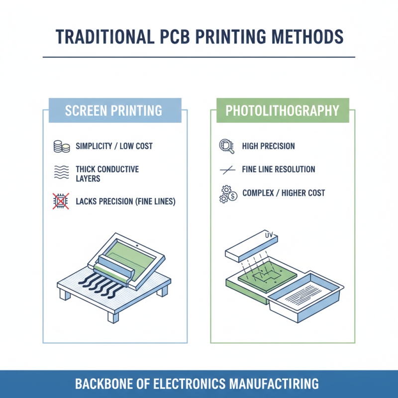
There are various methods, including screen printing, stencil printing, and inkjet printing. Screen printing, for example, remains popular due to its cost-effectiveness and ability to handle large volumes. However, it often lacks precision, especially with fine lines and small components. In contrast, inkjet printing allows for high-resolution outputs but can struggle with material compatibility and speed. In a recent industry survey, 58% of professionals noted that their choice of technique often resulted in trade-offs between speed and quality.
Evaluating these techniques requires a focus on specific project needs. Factors such as layer count and design complexity influence the choice. Often, designers face dilemmas. While they lean towards faster methods, they may compromise on fidelity. It's crucial to analyze each technique’s strengths and weaknesses carefully, as overlooking details can lead to significant consequences in PCB performance.
| Technique | Description | Application | Advantages | Disadvantages |
|---|---|---|---|---|
| Screen Printing | A stencil is used to apply ink onto the substrate. | Low to medium volume production. | Cost-effective for small runs. | Not suitable for fine details. |
| Digital Printing | Direct printing of designs using inkjet technology. | Prototyping and custom designs. | High detail and flexibility. | Higher cost per unit. |
| UV Printing | Uses ultraviolet light to cure ink as it is printed. | Custom graphics and quality finishes. | Immediate curing and durability. | Limited material compatibility. |
| Pad Printing | Transfer of ink to a substrate through a silicone pad. | Irregular shapes and curved surfaces. | Excellent for complex surfaces. | Limited to smaller designs. |
| Flexographic Printing | Uses flexible relief plates to print on a variety of substrates. | High volume production. | Fast and efficient for large runs. | Setup costs can be high. |
| Gravure Printing | Engraved cylinders transfer ink to the substrate. | High-quality and fine detail printing. | Excellent for high volume. | High initial setup cost. |
| Laser Printing | Uses laser technology for high precision printing. | Prototyping and detailed applications. | High accuracy and detail. | Rate of speed can be slower. |
| Offset Printing | Ink is transferred from a plate to a rubber blanket, then to the substrate. | High volume printing. | High-quality finishing. | Not cost-effective for small runs. |
| Conductive Printing | Printing of conductive materials to create electronic circuits. | Flexible and wearable electronics. | Innovative electronic solutions. | Limited to specific applications. |
| 3D Printing | Layered material deposition to create objects. | Prototyping and complex geometries. | Highly customizable designs. | Time-consuming for large volumes. |
High-quality PCB printing is crucial in electronics manufacturing. Poor printing techniques can lead to functional failures. When a PCB is printed with precision, it results in better connections and minimizes defects. This can significantly enhance the performance of electronic devices. Without attention to detail, small errors can create big problems, like circuit malfunctions.
One tip for improving PCB printing quality is to use appropriate materials. The choice of ink and substrate impacts the clarity of the printed circuits. Using outdated materials can result in a blurry or incomplete design. Regularly reviewing and upgrading materials can prevent such issues. Ensuring proper calibration of your printing equipment is another essential factor. Misaligned machines can create inconsistencies in your designs. This often requires frequent checks.
Understanding your design layout is also vital. Not all designs translate well into printed PCBs. Complex layouts may cause inaccuracies during the printing process. Trying simpler designs can often yield better results. Continuous testing and refinement of your printing technique are necessary. It’s not just about following a process; it’s about adapting to feedback and setbacks. Each print run is an opportunity to learn and improve.
Traditional PCB printing methods have been the backbone of electronics manufacturing for decades. Techniques like screen printing and photolithography dominate this space. Screen printing is popular due to its simplicity and low cost. It allows for the application of thick layers of conductive paste, which can be critical for certain applications. However, it often lacks precision, especially for fine lines, leading to issues in high-density boards.
In contrast, photolithography offers superior accuracy and detail. It uses light to transfer a geometric pattern from a photomask to a light-sensitive chemical. The result is high-resolution features that can reach sub-micron levels. Reports indicate that photolithography can achieve line widths under 5 microns, a stark contrast to the 100-micron limit often seen in screen printing. However, this method is generally more expensive and requires a more complex setup. As a result, manufacturers may face challenges regarding cost versus performance.
Many PCB production facilities still rely heavily on traditional techniques. A recent industry survey found that 65% of manufacturers would prefer older methods for prototyping due to lower initial costs. Yet, with the growing demand for miniaturization, there is pressure to adopt more advanced methods. Balancing cost and quality remains a significant challenge in the ever-evolving landscape of PCB manufacturing.
In recent years, the PCB printing industry has witnessed remarkable innovations. Emerging technologies, such as additive manufacturing and advanced ink formulations, are reshaping the landscape. According to a report by MarketsandMarkets, the global PCB market is expected to reach $90 billion by 2025, driven largely by these advancements.
Additive manufacturing, or 3D printing, is becoming increasingly popular. This method allows for complex designs and reduces material waste. Recent studies suggest that with 3D printing, manufacturers can save up to 50% on production costs compared to traditional methods. It also enables rapid prototyping, which shortens product development cycles significantly.
Tips: When exploring new PCB printing technologies, consider the compatibility of materials. Different inks react differently, affecting durability and performance. Conduct thorough testing before large-scale production.
Another emerging technology involves the use of conductive inks. These inks can be printed onto flexible substrates, leading to innovative applications in wearables and IoT devices. However, the reliability of these inks varies widely. Some may not withstand extreme conditions. Therefore, testing in real-world scenarios is crucial.
Tips: Always keep up with emerging trends in PCB technologies. Staying informed can lead to better decisions for future projects. Regularly evaluate your processes to find areas for improvement.
Achieving high-quality results in PCB manufacturing hinges on several best practices. One crucial factor is the selection of the right printing technique. According to a recent report, 75% of defects in PCBs arise from improper printing methods. Opting for techniques like screen printing or inkjet printing can significantly enhance the quality.
Screen printing provides robust ink adhesion and allows for thicker layers, while inkjet is known for its precision and flexibility.
Tips: Always test on a small scale before large runs. This will help identify any issues early. Calibration of printers is also vital. Regularly check and adjust settings to meet specific requirements.
The choice of materials impacts quality too. The substrate of the PCB should match the intended application. A mismatch can lead to failures or reduced lifespan. Industry standards recommend using high-grade materials for critical applications. However, some manufacturers still cut costs, leading to poorly performing boards.
Tips: Be aware of supplier certifications. Only work with reputable suppliers to ensure material quality. Conduct thorough inspections of materials before starting production. Small changes can lead to significant improvements in the end product.