2026 How to Design a Printed Circuit Board with Ease?
Designing a printed circuit board (PCB) is a nuanced task that embodies both art and science. As Dr. Sofia Chen, a renowned expert in PCB design, aptly stated, “The beauty of a printed circuit board lies in its complexity and precision.” In today's rapidly evolving technology landscape, mastering PCB design can be challenging yet rewarding. Engineers often underscore the importance of a meticulous approach.
While many struggle with layout and component placement, each step requires thoughtful consideration. Schematic design forms the backbone of an effective PCB, but it is not without its hurdles. Understanding electronic signals, managing space, and ensuring functionality are critical. Mistakes at this stage can lead to considerable redesign efforts.
Moreover, a modern PCB design solution must also factor in manufacturability. Inconsistent practices can lead to costly production flaws. As design complexity increases, the stakes are even higher. Reflecting on past projects may reveal instances of oversight, emphasizing the need for ongoing learning. Ultimately, anyone venturing into the PCB design realm should embrace both the challenges and joys of the process.
Understanding the Basics of Printed Circuit Board (PCB) Design
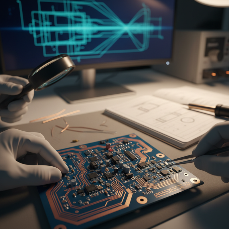
Understanding the basics of printed circuit board (PCB) design is crucial for anyone entering the field of electronics. A PCB connects various components, allowing them to communicate effectively. This connection is not trivial; it involves careful planning and precise execution. For a beginner, the intricacies of trace routing and spacing can feel daunting but are essential for reducing interference and ensuring a functional board.
Component placement is a vital part of PCB design. Each component must be positioned logically. It’s tempting to place them wherever there is space, but this often leads to inefficient layouts. Paying attention to signal flow helps. Thoughtfully arranging components can lead to better performance. It is also important to consider thermal management. Heat sinks might seem unnecessary at first, but they could prevent potential failure in high-current areas.
Moreover, using PCB design software can streamline this process. However, understanding the limits of your tool is equally important. Bugs can crop up unexpectedly. Modeling a design doesn’t always translate to a successful prototype. Testing and revisions are part of the learning experience. Mistakes offer valuable lessons in refining the design process. Embracing these challenges can significantly enhance your PCB design skills.
Key Tools and Software for Efficient PCB Design in 2026
In 2026, the landscape of PCB design has evolved significantly with advancement in tools and software. Key software solutions now integrate AI algorithms, assisting engineers in various design tasks. Reports suggest that over 70% of designers utilize simulation tools to minimize errors. These tools enable extensive analysis of electrical performance before prototyping.
Cloud-based platforms have gained traction. They promote collaboration and version control among teams. A study conducted by TechGear found that projects using cloud solutions saw a 30% reduction in lead times. However, despite these advancements, many designers still encounter challenges with circuit complexity. Approximately 58% of PCB designers express difficulty in managing multi-layer layouts effectively.
Additionally, design rule checks remain a crucial aspect. Automating these checks enhances reliability but can introduce new errors if not monitored closely. Engineers must remain vigilant in refining their processes. Adapting to new technologies is essential, yet it often requires an adjustment period. Embracing these tools while acknowledging their limitations will shape a more efficient PCB design process in the coming years.
Essential Design Principles: Components, Layers, and Trace Routing
When designing a printed circuit board (PCB), understanding essential design principles is crucial. Begin with the placement of components. Key factors include connection points and overall layout. Components should be spaced correctly to avoid overcrowding. This promotes better heat dissipation and easier soldering. Don’t underestimate the importance of a logical flow. An organized layout enhances performance and reliability.
Layers play a significant role in PCB design. A typical board may consist of multiple layers, such as signal layers, ground planes, and power planes. Each layer serves a purpose. For instance, ground planes reduce electromagnetic interference, improving signal integrity. However, managing layer transitions can be challenging. Designers must ensure that vias do not create unwanted inductance or resistance.
Trace routing is another critical aspect. Traces connect components and must be carefully designed. Keep trace lengths short to minimize resistance and potential signal loss. Use wider traces for high-current paths to prevent overheating. Remember, frequent trace bends can also cause issues. Balancing aesthetics and functionality can lead to design flaws. Reflect on your design choices to enhance future projects.
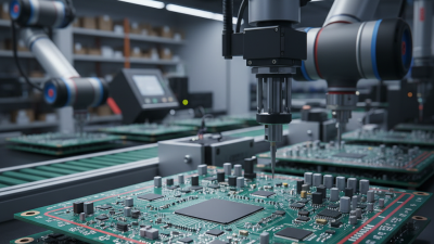
Manufacturing Process: From Prototyping to Mass Production
Designing a printed circuit board (PCB) requires a thorough understanding of the manufacturing process. It is crucial to focus on each stage, from prototyping to mass production. Prototyping usually involves creating a small batch of PCBs to test functionality. According to industry reports, nearly 70% of PCBs tested at this stage face design issues that need refinement. This emphasizes the importance of meticulous design reviews.
Mass production ramps up a PCB's complexities. The transition from prototype to mass production often leads to challenges in quality control. A study from the IPC (Association Connecting Electronics Industries) indicates that about 30% of PCBs produced at the mass level do not meet quality standards. This calls for precise communication between design teams and manufacturers. Quality assurance processes must be in place to reduce defects.
The global PCB market reached $60 billion in 2022, with an expected growth rate of 4.2% per year. Manufacturers must adopt advanced technologies to keep up. This includes automation in production lines and implementing rigorous testing protocols. Such innovations can greatly improve efficiency and reliability in PCB manufacturing, yet many companies struggle to integrate these technologies effectively. Continuous learning and adaptation are vital for success in the competitive PCB landscape.
2026 How to Design a Printed Circuit Board with Ease? - Manufacturing Process: From Prototyping to Mass Production
| Phase |
Duration |
Key Activities |
Tools & Techniques |
Cost Estimate |
| Concept & Design |
1-2 weeks |
Schematic creation, component selection |
CAD Software, Simulation Tools |
$500 - $1000 |
| Prototyping |
2-4 weeks |
PCB fabrication, assembly |
PCB Fabrication Services, Soldering Tools |
$2000 - $5000 |
| Testing |
1-2 weeks |
Functional testing, quality assurance |
Testing Equipment, QA Processes |
$1000 - $2000 |
| Mass Production |
4-12 weeks |
Large scale manufacturing, distribution |
Automated Assembly Lines, Supply Chain Management |
$10,000 - $50,000 |