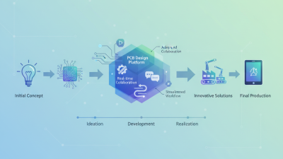
How to Design a PCB Board Step by Step?
A reliable pcb board design begins long before traces appear on the screen. It starts with clear requirements: board dimensions, connector locations, operating voltage, expected temperature, and the signals that need careful routing. Those details shape the schematic, component choices, and layer stackup. Rick Hartley, a respected signal-integrity educator, has repeatedly emphasized a practical point: a signal route must be considered together with its return path. That connection is easy to overlook. It can also affect noise, timing, and electromagnetic performance.
This guide follows the work step by step, from requirements and schematic capture to component placement, routing, and manufacturing checks. You will see why footprints should match their datasheets, why decoupling capacitors belong close to power pins, and why controlled-impedance traces need a suitable stackup. We will also cover design-rule checks, silkscreen details, and the files a fabricator needs. Small details matter. A board that looks neat on screen may still fail because of a swapped connector pin or an unsuitable clearance. No checklist catches everything; even experienced designers revisit assumptions after reviewing a prototype. Use the manufacturer’s current capabilities and component documentation as references, then inspect the design with fresh eyes before release. That final review is not busywork. It is where avoidable surprises often become visible.
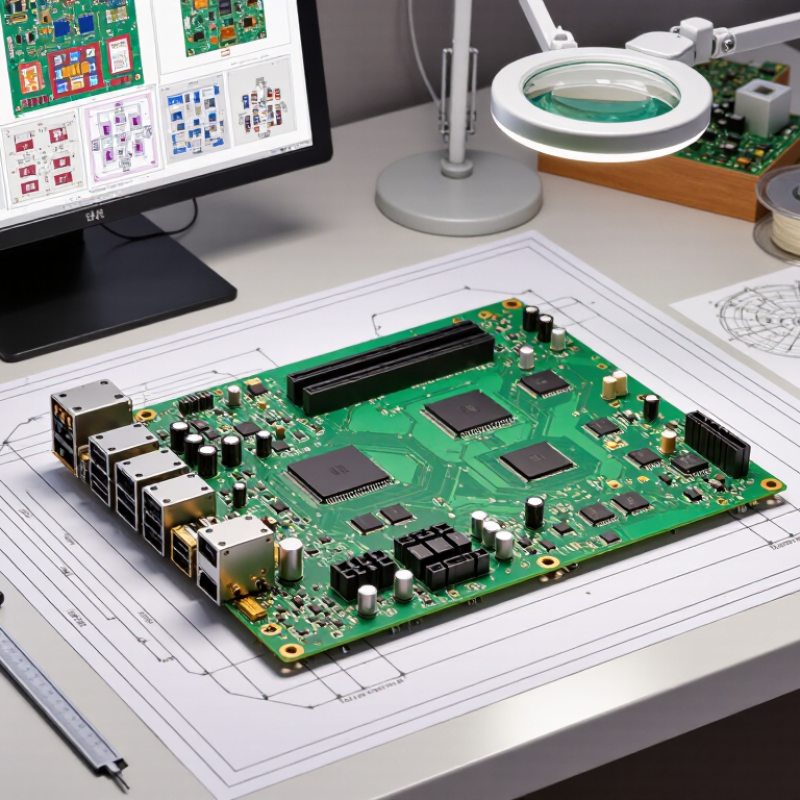
Establish Electrical Requirements and Create the Circuit Schematic
How to Design a PCB Board Step by Step?
Establish Electrical Requirements and Create the Circuit Schematic
Before drawing the schematic, define what the board must handle. Record each rail’s nominal voltage, tolerance, peak current, startup behavior, and expected load. For example, a motor output may draw 1.8 A briefly, even when its average current is much lower. Note signal levels, communication interfaces, connector pinouts, and operating temperatures too. These details guide component selection and prevent vague assumptions from becoming copper-routing problems. Keep a requirements table beside the schematic. Small effort, big payoff.
Translate each function into a clear circuit block: power input, protection, regulation, processing, and external connections. Add component values, reference labels, and net names as you draw. Place decoupling capacitors near the relevant power pins; a drawn connection does not guarantee a good physical layout. IPC-2221B defines three performance classes, helping designers align board design with the assembly’s reliability needs. For current-carrying traces, consult IPC-2152 rather than relying on a single rule of thumb; its guidance considers current, copper thickness, and temperature rise. Check every connector pin against its datasheet. I still find it easy to overlook startup current, so I mark that assumption for review. Keep the schematic readable, then run electrical-rule checks before layout.
Select Board Materials, Layers, and Component Footprints
Choose the board material around its real operating conditions, not habit. Standard FR-4 suits many general-purpose circuits, but temperature, moisture, signal speed, and assembly heat can change the choice. Check the laminate’s glass-transition temperature and dielectric properties against the design requirements. Then define copper weight and board thickness; these affect current capacity, impedance, and manufacturability. A few extra layers may simplify dense routing, but they also add cost. Keep the stack-up intentional.
The Global E-waste Monitor 2024, published by ITU and UNITAR, reports 62 million tonnes of e-waste generated worldwide in 2022; only 22.3% was documented as formally collected and recycled. That is a useful reminder to consider durability and repair access while choosing materials and layer count. A robust board is not automatically a sustainable one. This trade-off deserves more attention.
Footprints need equal care. Use the component manufacturer’s dimensions and the IPC-7351 land-pattern guidance, then check pad spacing, solder-mask openings, courtyard clearance, and assembly tolerances in the CAD library. For a fine-pitch package, inspect the pads at full scale; a tiny offset can cause bridging or weak joints. Add thermal vias only when the copper layout and assembly process support them. I still find connector clearance easy to underestimate, especially near enclosure walls. Print the layout at 1:1 scale and test-fit critical parts before release.
How to Design a PCB Board Step by Step? – Select Board Materials, Layers, and Component Footprints
| Step |
Design Decision |
Common Options or Values |
Practical Guidance |
| 1 |
Define electrical and mechanical requirements |
Board outline, operating voltage, current, temperature range, connectors, mounting points, and enclosure limits |
Record component locations and keep-out areas before routing. Check connector orientation and mounting-hole positions against the mechanical design. |
| 2 |
Select the base material |
FR-4 is common for general-purpose rigid boards; higher-temperature or specialized laminates may be needed for demanding thermal, frequency, or environmental requirements. |
Compare glass-transition temperature (Tg), dielectric properties, moisture behavior, and the assembly process. FR-4 properties vary by laminate; confirm the selected material’s datasheet. |
| 3 |
Choose the number of copper layers |
2 layers for simpler designs; 4 or more layers for denser routing, dedicated power/ground planes, or controlled signal routing. |
A four-layer stack commonly places signal layers on the outside and ground and power planes inside. Keep high-speed signals close to a continuous reference plane. |
| 4 |
Set board thickness and copper weight |
1.6 mm is a common finished thickness; 35 µm copper is approximately 1 oz/ft² nominal copper weight. |
Confirm available thicknesses with the fabricator. Select copper weight and trace width based on current, allowable temperature rise, layer location, and manufacturing rules. |
| 5 |
Choose component footprints |
Through-hole and surface-mount packages; pad dimensions depend on the component package and assembly requirements. |
Use the component datasheet’s package dimensions and pin numbering. Verify pad pitch, pin-1 orientation, exposed pads, courtyard, and solder-mask openings before placement. |
| 6 |
Plan placement and routing |
Group functional blocks; keep decoupling capacitors close to power pins; provide short return paths for fast signals. |
Place connectors and mechanical parts first. Keep noisy switching or high-current paths away from sensitive analog circuits, and avoid splitting a reference plane beneath critical signals. |
| 7 |
Apply design rules and verify the layout |
Clearance, trace width, drill size, annular ring, solder-mask clearance, and edge spacing are set by design needs and fabricator capabilities. |
Run electrical and design-rule checks, inspect the 3D or mechanical view, and review the fabrication outputs. Confirm the final rules with the chosen manufacturing process. |
Note: Values shown are common reference points, not universal requirements. Final material choices, stack-up, dimensions, and manufacturing limits should be verified against the design requirements and fabricator specifications.
Arrange Components and Define the Board Layout
Place components by function, not by visual symmetry. Keep connectors along board edges, then group the power stage, processor, and communication circuits. Put each decoupling capacitor close to its IC power pin; a short, direct path reduces unwanted loop area. Leave room for the mounting holes and the screwdriver that must reach them. It is easy to miss that detail.
Before routing, sketch the major signal paths and mark noisy switching nodes. Separate sensitive analog inputs from fast clocks and power converters. IPC-2221B, an industry design standard, bases conductor sizing on current, copper thickness, and allowable temperature rise—not one universal trace width. Check those inputs against your actual stack-up and fabrication limits. The standard is guidance, not a substitute for review.
Tips: Reserve test points and keep copper clear of board edges and hardware. For a two-layer prototype, place ground continuity ahead of cosmetic alignment. Then inspect the layout at full scale: can parts be soldered, probes attached, and connectors accessed? This check often catches awkward placement. I still find that a neat screen view can hide a cramped physical corner.
Route Traces and Add Power, Ground, and Thermal Features
After placing components, route power and ground before low-level signals. Keep high-current paths short, wide, and direct; every extra bend adds resistance and complicates inspection. IPC-2152 guidance relates trace capacity to copper thickness, board material, and allowable temperature rise, so a single “safe” width does not fit every design. Check the current against the stack-up, then verify the result with a calculator or thermal test. That first pass is rarely right.
Use a continuous ground plane where possible, and avoid splitting return paths beneath fast signals. A detour around a plane gap can enlarge the current loop and increase noise. Add stitching vias near layer changes, but do not place them blindly; confirm they connect the intended ground regions. IPC’s 2023 industry data valued global PCB production at about US$70 billion, reflecting how widely boards serve products with very different power and thermal demands. The number is context, not a routing rule.
For heat, connect hot components to copper pours and thermal vias, then check whether the enclosure can release that heat. A dense via pattern beneath a power device may help, but it can also draw solder away during assembly. I sometimes leave more copper than calculations suggest, then reconsider after reviewing airflow and temperature measurements. Small details matter. Label test points and keep critical traces visible in layout reviews; an elegant route is not useful if nobody can verify it.
Check the Design and Export Manufacturing Files
Before exporting manufacturing files, inspect the board as if you were the fabricator receiving it. Run design-rule checks, then compare the PCB against the schematic netlist to catch missing connections and unintended shorts. Zoom in on tight-pitch pads, via clearances, board edges, and silkscreen text. A clean 3D view helps, but it cannot prove electrical connectivity. Confirm layer names, stackup thickness, copper weights, drill sizes, and soldermask openings against the fabrication notes. IPC-2221 provides widely used guidance for PCB design; your fabricator’s process limits still matter.
The Printed Circuit Board Market Size, Share & Trends Analysis Report from Grand View Research estimated the global PCB market at USD 76.1 billion in 2023 and forecast 5.6% annual growth from 2024 to 2030. A growing market makes clear handoffs more important, not less. Export Gerber X2 or IPC-2581 data, plus NC drill files and a readable fabrication drawing. Open the exported files in an independent viewer. Check that the board outline, plated holes, and copper layers appear in the right places. I still find that a polished layout can hide a careless file export.
Tips: Include the revision number in every file name. Keep a PDF drawing beside the fabrication package, and state units explicitly. Ask the manufacturer to review unusual via sizes or impedance requirements before production. Small detail. Big difference.