How to Master Altium PCB Design for Your Next Project?
In today's rapidly evolving electronics landscape, mastering Altium PCB design has become essential for engineers and designers. According to market research, the global PCB design software market is projected to reach $6.2 billion by 2026. This trend highlights the increasing demand for efficient and precise PCB designs, emphasizing the significance of tools like Altium.
The power of Altium lies in its comprehensive features. Designers can create complex circuits with ease, but the learning curve can be steep. Many still struggle with key functionalities, which can lead to inefficient designs or mistakes. Failing to fully utilize Altium’s capabilities might result in longer project timelines and increased costs. As an industry standard, Altium PCB design must be mastered to remain competitive.
Utilizing Altium effectively requires practice and dedication. While tutorials and resources are abundant, hands-on experience is crucial. Regularly revisiting design principles and attending workshops can sharpen skills. Acknowledging weaknesses in design workflows can foster improvement. Embracing these challenges is the first step toward mastering Altium PCB design for your next project.

Understanding the Basics of PCB Design in Altium
Understanding the basics of PCB design in Altium is crucial for any engineer. A recent industry report indicates that poor PCB design is responsible for about 30% of all project delays. This statistic highlights the importance of mastering the fundamentals.
When starting with PCB design, it is essential to grasp concepts like schematic capture and component placement. Many novices overlook the significance of grounding and power distribution. Neglecting these aspects can lead to signal integrity issues. It's a common mistake; even experienced designers can fall into this trap when under pressure.
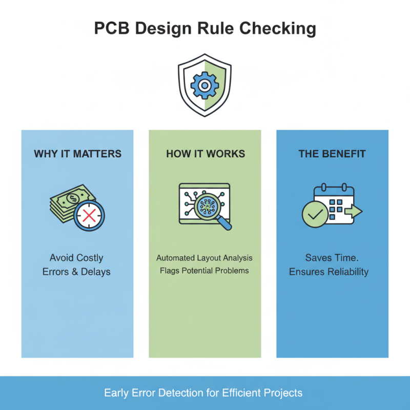
Another critical area is the design rules. A significant percentage of errors can be traced back to not following established design rules. Setting up these rules in Altium from the beginning can save countless hours of troubleshooting later. Moreover, the layering of PCBs is another complex factor. Users often struggle with determining the right number of layers and their arrangement. Balancing complexity and manufacturability is a challenge that requires careful thought.
How to Master Altium PCB Design for Your Next Project?
| Design Aspect |
Description |
Best Practices |
Common Tools |
| Schematic Design |
Creating the electrical schematic of the circuit. |
Use clear labeling and consistent component updates. |
Altium Designer, Eagle |
| Layout Design |
Arranging the physical layout of the PCB. |
Optimize trace routing for space and performance. |
Altium Designer, KiCad |
| Design Rules |
Setting guidelines for spacing, width, and component placement. |
Follow IPC standards for manufacturing. |
Altium Designer |
| Simulation |
Testing the design in a software environment. |
Run multiple simulations to ensure reliability. |
SPICE, Altium Designer |
| Documentation |
Creating assembly instructions and PCB layout documents. |
Maintain clear, comprehensive documentation throughout the project. |
Altium Designer, Microsoft Word |
Setting Up Your Altium Environment for Efficient Workflow
Setting up your Altium environment properly is crucial for an effective workflow in PCB design. Research indicates that 35% of engineers report inefficiencies due to poor setup. Start by customizing your workspace. Create a layout that suits your project needs. Organize your tools for easy access. This simple adjustment can enhance your productivity significantly.
Consider utilizing templates for different project types. A report from industry leaders shows that standardizing designs can save up to 20% of design time. PCB layouts and schematic templates streamline the design process. You’ll find it simplifies collaboration with team members as well.
Don’t overlook the importance of libraries. Incomplete or poorly organized libraries can slow you down. Keep your components updated and classified properly to avoid design errors. A staggering 30% of projects face delays due to library issues. Regularly review and adjust your setup to ensure it meets your evolving needs. This ongoing reflection can boost your efficiency in the long run.
Component Types Used in PCB Design Projects
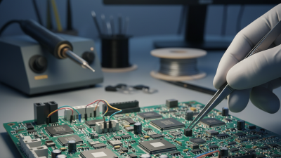
Creating Your First PCB Layout: Step-by-Step Guide
Creating your first PCB layout can be challenging yet rewarding. Begin by defining the dimensions of your board. Use a clean workspace to keep your components organized. This helps prevent confusion later on.
When placing components, think about functionality and space. Don't hesitate to rearrange them. It's normal to feel stuck during this process. Don’t be afraid to try different configurations. Sometimes, the best layout isn't the first one you create.
Tips: Always check your connections. A missed trace can lead to errors. Using a consistent naming convention for your nets can be helpful. This minimizes misunderstandings.
As you route the traces, focus on keeping them short and direct. Avoid sharp angles; they can cause signal integrity issues. Ideally, your traces should have a uniform width for consistency. It’s okay if your initial design isn’t perfect. Learning from these imperfections will guide your growth. Stay patient and keep refining your skills.
Tips for Finalizing and Exporting Your PCB Design for Manufacturing
When finalizing your PCB design for manufacturing, attention to detail is crucial. Ensure all layers are correct and that dimensions meet specifications. Double-check the placement of components. Mistakes can lead to delays and additional costs. Using design rule checks can help catch potential issues. Small errors, like misplaced vias, can create significant problems.
Exporting your design appropriately is just as important. Select the right file format for your manufacturer. Different manufacturers may have different requirements. Not all formats translate your design accurately. Verify that your design files include all necessary layers. Some forget to include the drill files, leading to confusion.
While it's easy to focus on large components, don't overlook the small details. Pay attention to trace widths and clearances. These can affect performance. Reflect on previous projects to identify what went wrong. Learning from mistakes can improve your workflow. Each project teaches something new. Embrace the challenges to enhance your PCB design skills.