How to Master PCB Board Design for Beginners and Professionals?
In the fast-evolving world of electronics, mastering PCB board design is essential for both beginners and professionals. According to a report by the IPC, the global PCB market is projected to reach $80 billion by 2026, reflecting the growing demand for smart devices and interconnected systems. This trend emphasizes the need for high-quality PCB board design skills. As expert John Smith, a well-known PCB designer, once stated, “A great PCB design is the foundation of a successful electronic product.” His insight highlights the critical role that PCB design plays in product development.
However, the journey into PCB board design is not without challenges. Many novices struggle with layout optimization and component placement, leading to potential errors. Learning the nuances of design software can be overwhelming. For professionals, staying updated on technological advancements and material innovations is crucial. The industry often shifts rapidly, and complacency can lead to missed opportunities.
By engaging with both foundational principles and advanced techniques, individuals can enhance their PCB board design skills. Effective design requires continual learning and adaptation. With commitment and practice, mastery is attainable. The road may have bumps, but each step brings valuable insights.
Understanding the Basics of PCB Design: Key Concepts and Terminology
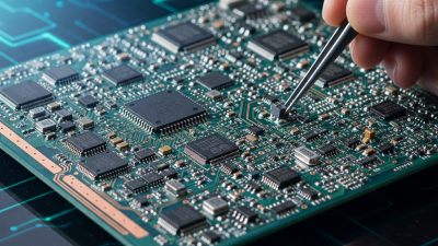
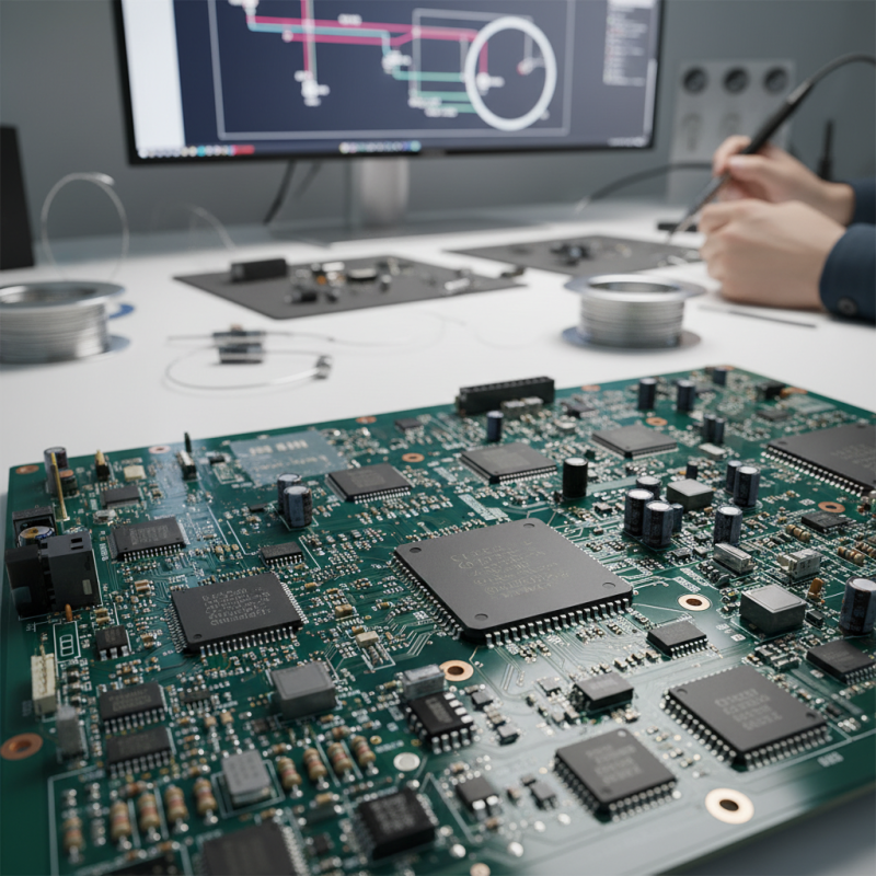
Understanding the basics of PCB design is crucial for anyone entering this field. A printed circuit board, or PCB, connects electronic components. The layout must be precise. Every line and space matters. Mistakes can lead to non-functional devices.
Key concepts include schematic diagrams and layouts. A schematic outlines the electrical connections. It shows how parts interact. Meanwhile, a layout places these components on the board. This step involves careful consideration. Each trace can affect signal quality. Always account for power distribution.
Terminology also plays a significant role. Terms like "trace," "pad," and "via" are essential. A trace conducts electricity. Pads are for component connections. Vias allow signals to pass through layers. Keeping these definitions straight can be challenging. It's common to mix them up at first. Learning from errors strengthens understanding. Embrace the process.
Essential Tools and Software for PCB Design: A Beginner's Guide
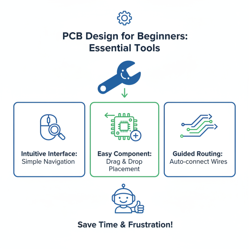
When starting with PCB design, choosing the right tools is crucial. You’ll come across various software options, each with unique features. Look for intuitive interfaces that simplify complex tasks. A beginner-friendly tool can save time and frustration. It helps if the software allows for easy component placement and routing.
Tools can range from basic to advanced. Simpler applications may lack advanced simulation features. However, they are often easier to learn. Professionals might need more sophisticated software to conduct extensive simulations. Meanwhile, beginners can focus on layout and design basics first. Analyzing what you truly need is important.
Tips: Regularly practice with your chosen software. Explore tutorials to understand functionality deeply. Don't hesitate to seek community support for troubleshooting. Mistakes in layouts are common. Learn from them rather than getting discouraged. PCB design requires iteration. Embrace the learning curve. Keep refining your skills, and experiment with different designs to grow your expertise.
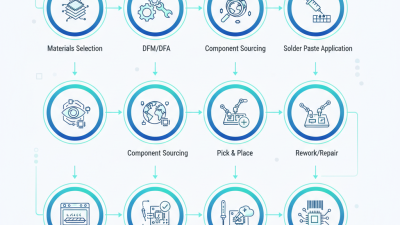
Step-by-Step Process for Designing Your First PCB Board
Designing your first PCB board can be both exciting and daunting. Begin by defining your project clearly. What do you want your PCB to achieve? Sketch your idea on paper. Visualizing helps in understanding component placement and board size. Keep it simple at first. Aim for fewer components to reduce complexity.
Next, choose a PCB design software. Many options are available, but the interface varies widely. Take time to explore the features. Watch tutorials if needed. Creating a schematic is your next task. Ensure your connections are correct. It is easy to make mistakes here. Double-check your work. Mistakes can lead to unexpected results.
After the schematic, move on to layout design. Arrange components thoughtfully. Space them out to avoid overlaps. This step can be frustrating; it often requires several adjustments. Be patient and expect to redo parts. Finally, create Gerber files for production. Review everything carefully before moving forward. Remember, PCB design improves with practice. Reflect on what went well and what went wrong. Each design teaches valuable lessons.
Best Practices for PCB Layout: Tips for Enhancing Performance
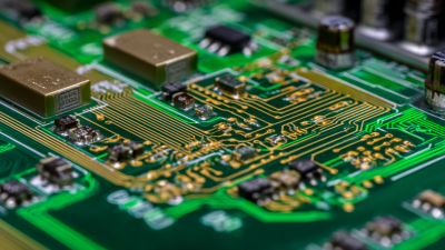
When designing a PCB, the layout is crucial for performance. According to industry reports, approximately 30% of PCB failures stem from poor layout choices. A well-thought-out design minimizes interference and signal crosstalk. This is essential, especially in high-speed circuits where precision matters.
One practice involves maintaining short trace lengths. Longer traces can introduce delays and noise. The IPC-2221 standard highlights that keeping traces under 1 inch can significantly improve signal integrity. Designers should also consider using a ground plane to reduce electromagnetic interference. Using the right layer stack-up and via placements can also enhance board performance.
However, it's easy to overlook small details. Ignoring component placement can lead to heat issues later. A cluttered layout often complicates troubleshooting. Regularly revisiting your layout strategy ensures continual improvement. Understanding these nuances is vital for both beginners and seasoned professionals in ensuring reliable PCB designs.
Troubleshooting Common PCB Design Issues: Solutions and Tips
Troubleshooting common PCB design issues can be daunting. Many beginners struggle with layout errors. According to a 2022 IPC report, 30% of PCB failures occur during the design phase. Careful attention to details is crucial. Components may be incorrectly placed, leading to signal integrity problems.
Heat dissipation is another common issue. Designers often overlook thermal management. Poor heat distribution can cause board failures. A study found that 25% of PCB defects were related to inadequate thermal design. To avoid these pitfalls, simulate thermal performance. Tools like thermal modeling software can help identify hotspots early.
Lastly, don't underestimate the importance of clear documentation. Inconsistent labeling can result in assembly errors. Research shows that 20% of production delays stem from poor communication. Keep layouts organized and ensure everything is well-documented. Regular reviews can lead to better outcomes. Clear visuals help convey complex designs effectively. Making these changes can significantly reduce errors and improve overall efficiency in PCB design.