How to Master PCB Design for Efficient Production?
In the rapidly evolving world of PCB design, efficiency is key. Renowned expert Dr. Emily Chen, a leading voice in electronics engineering, once stated, "Effective PCB design is the foundation of successful product development." Her insight echoes the importance of mastering the nuances in the design process.
PCB design is not just about aesthetics; it involves technical precision and strategic planning. Every component placement and trace routing affects the final product's performance. This complexity can lead to mistakes if not handled with care. For instance, poor layout can result in electrical interference, compromising device functionality. These pitfalls reveal that even experts must continually refine their skills and adapt to new technologies.
Attention to detail is crucial. Simple design flaws can lead to costly production delays. Thus, embracing a mindset of continuous learning in PCB design is essential for engineers. They must reflect on past projects and use lessons learned to enhance their future designs. The journey to mastering PCB design is ongoing, filled with challenges, yet rewarding for those willing to invest the effort.

Understanding the Basics of PCB Design Principles
Understanding the fundamentals of PCB design is essential for creating effective and efficient circuits. A good design should balance functionality and manufacturability. Designers often overlook the importance of layout symmetry. This can lead to signal integrity issues and increased production costs.
Component placement is critical. Placing components too close together can create thermal problems. Inefficient routing can also complicate manufacturability. It's vital to consider access for soldering and inspection. Many designers skip this step and face issues during production down the line.
Designers must work with appropriate layer stacking and impedance control. Ignoring these aspects can lead to signal loss and malfunction. It’s a common mistake to overlook design rules while focusing on innovative features. Striking a balance between creativity and practicality is essential for successful PCB design.
Key Factors Influencing Efficient PCB Production
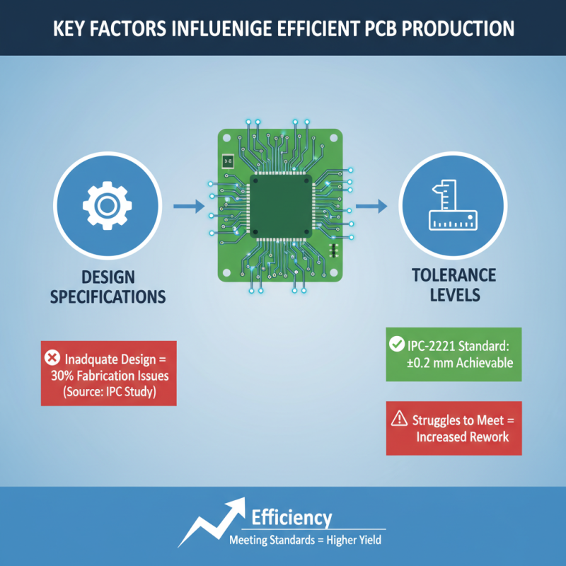
In the world of PCB design, several key factors influence production efficiency. Meeting tolerance levels is critical. The IPC-2221 standard states that a tolerance of ±0.2 mm is often achievable. However, many designs struggle to meet these standards, leading to increased rework rates. According to a study by the IPC, nearly 30% of PCB fabrication issues are linked to inadequate design specifications.
Another crucial factor is component placement. Optimal placement reduces trace lengths and improves signal integrity. Research indicates that rearranging components can decrease production time by up to 25%. Yet, designers frequently overlook this, resulting in longer assembly times and higher costs. A well-arranged PCB layout can enhance thermal management, thus addressing issues such as overheating and component failure during operation.
Additionally, the choice of materials impacts both performance and manufacturability. High-frequency materials may provide better signal integrity but often come with a higher price tag. The latest materials might not be suitable for all applications. Designers must balance cost and performance while ensuring compliance with industry standards. A study revealed that 40% of cost overruns were due to unexpected material issues. Efficient PCB production thus requires careful consideration of design principles, material selection, and ongoing attention to specification compliance.
Choosing the Right Tools for PCB Design Optimization
Choosing the right tools for PCB design optimization is crucial in today's fast-paced electronics industry. According to IBISWorld, the PCB industry grew by 3.6% from 2022 to 2023, highlighting the increasing demand for efficient design solutions. Selection of design software significantly impacts production efficiency and cost. Tools that integrate simulation capabilities can reduce errors in the design phase, which is paramount. Approximately 30% of PCB design errors arise from inadequate simulations.
However, not all tools are created equal. Some software may seem user-friendly but lack advanced features. A Study by ResearchAndMarkets notes that about 40% of engineers feel constrained by their design tools. They report the need for enhanced customization options and better collaboration features. Failing to choose the right software can lead to production delays, wastage of materials, and increased costs. Designers often overlook the importance of tool compatibility with manufacturing processes. This oversight can result in significant bottlenecks.
Incorporating reliable tools into your workflow requires careful assessment. Engineers should evaluate software based on user reviews and case studies. Engaging with community feedback can help identify practical challenges before investing time and resources. The effectiveness of a tool often lies in its adaptability to specific project needs. A thoughtful selection process can substantially improve the overall design efficiency and production timeline. It is essential to remain reflective about these choices.
PCB Design Tools Efficiency Comparison
Best Practices for Component Layout and Placement
Effective component layout and placement are crucial for PCB design. While it may seem straightforward, many designers overlook small details that lead to larger issues. For instance, placing components too close can cause interference. Consider the flow of signals. Ensure that critical components, such as ICs and capacitors, are positioned near their connections. This limits the length of traces and reduces noise.
Tips: Always account for thermal management. Spread out heat-generating components to avoid overheating. Use thermal vias to direct heat away.
Another common error is neglecting the importance of layout symmetry. An unbalanced layout can lead to signal integrity issues. Staggering components in a more orderly fashion improves both performance and manufacturability.
Tips: Think about accessibility. Components near the edges are easier to solder. Position push buttons and connectors accordingly for user interaction.
Reflection on these practices reveals that the smallest choices matter. Each decision impacts the final product's performance and reliability. Balancing aesthetics with function is essential. Embrace iterative design and feedback for continuous improvement.
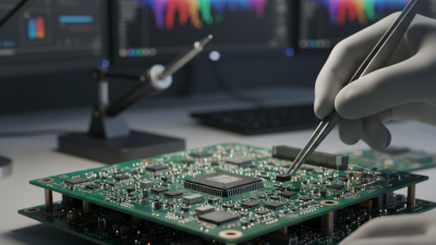
Testing and Iteration: Ensuring Quality in PCB Production
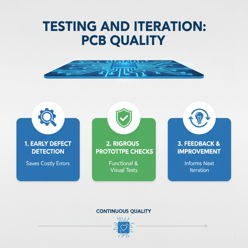
Testing is a crucial phase in PCB production. It helps identify defects early on. Without thorough testing, issues may go unnoticed until later stages, leading to costly errors. Each prototype must undergo rigorous testing. Functional tests check if the PCB behaves as expected. Visual inspections reveal physical anomalies. Both methods provide valuable feedback for further iterations.
Iteration is equally important. After the initial tests, insights will guide improvements. Designers should refine layouts based on test outcomes. Sometimes, the initial design may not meet thermal or signal integrity requirements. It is necessary to adjust components and reroute traces. This iterative approach fosters a culture of continuous improvement.
A flow of feedback between production and testing also enhances reliability. Communication ensures that engineers understand problems. It also allows them to verify if changes solve identified issues. Even with thorough testing, unexpected failures may arise later in production. It’s vital to keep learning from each iteration and adapt accordingly. Embracing imperfections can lead to stronger, more reliable PCB designs.