Learning PCB design can feel abstract until a circuit becomes a board you can inspect. A good pcb design course turns that gap into practical steps: reading a schematic, placing components, routing traces, and checking the finished layout. Beginners should also learn what common tools can and cannot verify. A clean-looking screen is not proof of a reliable board.
PCB design educator Rick Hartley often stresses the importance of return-current paths. As he puts it, “There are no signals without return currents.” This principle helps explain why ground planes, trace routing, and component placement matter. Small details matter.
A beginner-focused course should connect those details to real design decisions. Expect lessons on footprints, design rules, copper layers, and basic manufacturing files. A simple LED board can make these ideas tangible: you can follow each connection, inspect the ground return, and spot a misplaced connector before ordering anything. The best courses include guided projects, clear explanations, and chances to revise mistakes. Yet no course makes every design choice obvious. I would not pretend otherwise. Learners still need patience, careful checking, and feedback from experienced designers. This guide will compare online options by teaching approach, project depth, software access, and beginner support, so you can choose a practical starting point.
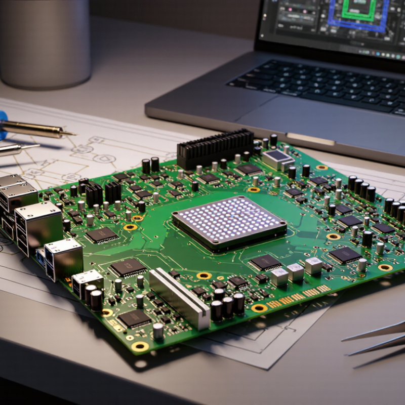
PCB design turns an electrical plan into a physical board that connects components through copper traces. A designer starts with a schematic, then arranges parts and routes their connections across one or more layers. The layout must leave room for components, soldering, and mounting holes. Trace width matters; it depends on factors such as current and copper thickness. Spacing also matters, both for reliable fabrication and electrical performance. Small details matter.
Beginners study PCB design to understand how circuit decisions affect real hardware. Moving a capacitor closer to a chip, for example, can improve its usefulness in a circuit. Learning to read design-rule warnings helps students catch issues like unconnected pins or insufficient spacing. These checks are helpful, but they do not prove that a board will work as intended. Careful review and testing remain important. Early layouts can look tidy on screen and still feel cramped when assembled. That mismatch is worth noticing. Practice teaches learners to compare the schematic, board layout, and physical prototype, then revise what did not work.
Top PCB Design Courses Online for Beginners
Learning PCB design starts with a few dependable habits, not a crowded tool list. Beginners should learn how components connect in a schematic before arranging them on a board. Practice reading resistor values, identifying pin numbers, and tracing signal paths between parts. Small steps matter. A simple LED circuit can teach these skills without hiding the basics behind a complex project. Check each component’s datasheet for its footprint, pin spacing, and operating limits. These details prevent common layout mistakes.
A beginner course should introduce schematic capture, board layout, and basic design-rule checks. Learn how board edges, copper layers, trace widths, and clearances affect a finished circuit. A ruler and graph paper can help with early placement sketches; design software is needed for building and checking the actual board files. Mistakes are useful. A trace that is too narrow or a connector placed too close to an edge can reveal what a rule is protecting against. Some lessons may make routing look cleaner than it feels in practice. Pause, inspect the connections, and revise one section at a time. Keep a small project notebook with design choices and questions to revisit.
| Learning Module | Core Skills Covered | Tools and Concepts | Beginner Practice Project | Typical Self-Paced Time |
|---|---|---|---|---|
| Electronics and PCB Foundations | Read simple circuit diagrams, identify common components, and understand voltage, current, resistance, and polarity. | Basic circuit symbols, resistor color codes, datasheets, and a digital multimeter. | Identify components and check a simple low-voltage circuit against its schematic. | 2–4 hours |
| Schematic Capture | Place symbols, connect nets, label signals, and organize a readable circuit schematic. | Schematic editor, component symbols, net labels, and electrical-rule checks. | Draw a schematic for a basic LED circuit with a current-limiting resistor and power input. | 3–5 hours |
| Components and Footprints | Match schematic symbols to physical packages and check pin numbering, dimensions, and spacing. | Component datasheets, footprint libraries, package drawings, and pin maps. | Select suitable footprints for the LED, resistor, and connector in the practice circuit. | 2–4 hours |
| Board Layout Basics | Set board shape, place components, plan signal flow, and route tracks while keeping connections organized. | PCB layout editor, copper layers, track width, clearance, vias, and ground connections. | Lay out a small, single-sided LED board with clear component placement and routing. | 4–6 hours |
| Design Rules and Review | Find common layout errors and verify that the board matches the schematic. | Design-rule checking, connectivity checks, clearance rules, and visual inspection. | Run rule checks on the practice board and correct unconnected nets or spacing violations. | 2–3 hours |
| Manufacturing Files and Assembly | Prepare a design for fabrication and understand the information needed for board assembly. | Gerber files, drill files, board outline, solder mask, silkscreen, and bill of materials. | Generate a manufacturing-file set and review the layers and component list before submission. | 2–3 hours |
| Capstone: Simple Functional Board | Combine schematic capture, footprint selection, placement, routing, rule checking, and file export. | PCB design workflow, datasheet review, design rules, and manufacturing outputs. | Complete a small low-voltage board, such as an LED indicator board with a connector. | 5–8 hours |
Time ranges are approximate self-study estimates and vary with prior electronics experience and project complexity.
Top PCB Design Courses Online for Beginners
When comparing online PCB design courses for beginners, look beyond the course title. Check whether lessons teach schematic capture, component selection, board layout, and design-rule checks in a clear sequence. A useful course shows real screens, not only polished diagrams. Look closely. Can you follow a small project from circuit idea to exported manufacturing files? Check the software requirements, lesson length, and whether practice files are included. Also review the instructor’s engineering background and the course update date; interfaces and workflows can change.
Tips: Read the sample lesson before enrolling. Look for exercises that include a simple sensor board, a parts list, and feedback on common errors. Confirm that questions receive specific answers.
A beginner-friendly course should explain why trace width, clearance, and ground placement matter, not just where to click. It should also show how to inspect a board in 3D and resolve basic rule violations. Compare course projects with your own goals, such as making a small controller or learning layout fundamentals. Reviews can help, but weigh detailed comments more than star ratings alone. I still find that a course can seem clear until the first design error appears. Choose one that makes room for revision, because that is where much of the learning happens.
Popular online PCB design courses usually combine short lessons, guided software practice, and small board projects. Beginners may draw a schematic, place a connector, and route power and signal traces. Strong courses explain why trace width, clearance, and ground planes matter, not just which buttons to click. Some include design-rule checks and 3D previews, helping learners spot a misplaced mounting hole before preparing a board. That detail helps. Lessons on schematic reading and component datasheets are useful too, because layout choices depend on electrical limits.
Look for downloadable practice files, clear notes, and exercises that progress from a simple LED board to a small sensor circuit. Feedback matters. Instructor reviews or peer critique can expose confusing labels and awkward connector placement. Courses that cover manufacturing files, such as Gerber and drill files, show how a digital design becomes a physical board. A bill of materials is another practical feature. Good lessons demonstrate common fixes, including correcting a wrong footprint or reconnecting an unconnected net.
Still, recorded videos may leave learners guessing when their own project behaves differently. Even polished courses can make PCB work look tidier than it is; a connector may shift, or a trace may need rerouting. Treat a certificate as a milestone, not proof of skill. Rebuilding a small board can reveal more.
Top PCB Design Courses Online for Beginners
Choose a course by the board you hope to make, not by its “beginner” label. A hobby project may need basic schematic capture, component footprints, routing, and design-rule checks. A path toward professional work may also require stack-up planning, signal integrity, and manufacturing handoff. Be specific. “Learn PCB design” is a vague goal; “route a small sensor board” gives you a useful test.
Read the syllabus and inspect the projects before enrolling. Look for practice files, clear explanations of library parts, and exercises that progress from a schematic to fabrication outputs. Check whether lessons explain why a clearance or trace width matters, rather than only which button to press. Instructor experience and recent course updates can help, but a certificate alone says little about practical skill. It is easy to overvalue polished videos. A modest course with thoughtful feedback may teach more. I would still check whether its pacing fits your schedule; that detail is easy to overlook.
Tips: Match the course project to your goal. Confirm software requirements and lesson update dates. Try a sample lesson, if available. Notice where you get stuck. That is useful evidence, not failure. If you want guided support, check how questions are answered before committing.
Suggested priorities when comparing courses. These are editorial recommendations, not survey results.
Look for hands-on projects first, then a clear schematic-to-layout workflow. Design-rule checks and fabrication-ready file exports help connect design practice to real-world PCB production.