What Is Prototype PCB Assembly and How Does It Work?
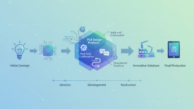
A circuit can look complete on a screen and still fail on the bench. That gap is where prototype PCB assembly becomes useful. It turns a board design into a physical unit that engineers can power, inspect, and revise before committing to larger production runs.
The market context is moving quickly. In its Fall 2024 forecast, the World Semiconductor Trade Statistics (WSTS) organization projected global semiconductor sales of $627.6 billion in 2024 and $697.2 billion in 2025. These figures measure semiconductor sales, not PCB assembly demand. Still, they underline why early hardware validation matters as electronic designs grow more capable and complex. A prototype helps teams test component fit, electrical behavior, and manufacturing choices while changes remain manageable.
In practical terms, prototype pcb assembly involves preparing a small quantity of boards, sourcing components, placing them, and soldering them using suitable production methods. The work may include surface-mount devices, through-hole parts, or both. Engineers then check the assembled board through visual inspection and functional testing. A tiny resistor can sit crooked; a connector can obstruct a nearby component. Small details matter. IPC standards such as IPC-A-610 and J-STD-001 provide recognized criteria for electronics assembly and soldering, though teams must select requirements suited to their product. A prototype is not a guarantee of production success. It is evidence, and sometimes inconvenient evidence, that exposes design or process assumptions before they become expensive. Understanding each assembly stage makes those lessons easier to act on.
What Defines Prototype PCB Assembly and Its Low-Volume Role
Prototype PCB assembly is the small-scale production of circuit boards built to test a design before larger manufacturing runs. It combines bare-board fabrication with component placement, soldering, and basic inspection. Prototype orders may range from a single board to a few dozen, depending on the project and assembly process. Not mass production.
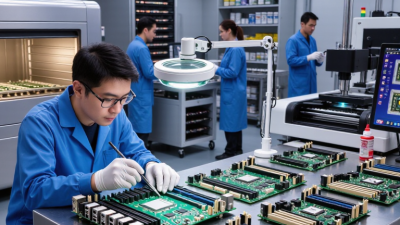
This low-volume role helps engineers check whether a design works beyond the screen. A test board can reveal misplaced components, awkward connector access, or solder joints that need closer inspection. Assemblers may use solder paste and a stencil, place components by hand or machine, then reflow the board in a controlled oven. For a tiny run, some steps may be manual, which can affect repeatability.
A prototype is also a practical way to examine assembly risks. For example, a connector placed too close to a board edge may be difficult to solder or handle. Inspection can include visual checks, power-on testing, and measurements at key points. These checks find problems, but they do not prove that every board will perform reliably over time. Even a board that works once can expose a weakness only after repeated testing. That uncertainty is easy to underestimate. Changes between prototype revisions should be recorded carefully, or test results may no longer match the board being evaluated.
Prototype PCB Assembly: From First Build to Production
Prototype PCB assembly turns a small batch of bare circuit boards into assembled boards for design verification and testing. The quantities shown are illustrative examples, not industry standards: actual order sizes vary by project, supplier, and product. Low-volume builds help teams find issues and refine a design before scaling up.
How BOM, Gerber Files, and IPC-2221 Guide Board Preparation
Prototype PCB assembly begins by turning design data into a buildable board and a clear parts list. The BOM identifies each component by reference, value, package, and specification. A vague entry can lead to a substitution that changes fit or performance. Gerber files describe copper, solder mask, and silkscreen layers; drill data defines hole locations and sizes. Check that filenames, revisions, and layer outputs match before release. One mismatch can place a label beneath a component or shift a footprint.
Tips: Compare BOM reference designators with the silkscreen and placement data. Open the Gerbers in a viewer and inspect fine-pitch pads, board edges, and drilled holes. Keep one revision number across every file. Small gaps matter.
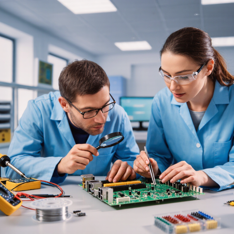
IPC-2221 provides general guidance for PCB design, including conductor spacing, clearances, and layout considerations. It helps teams assess whether a design is practical, but it does not replace checking the fabricator’s capabilities or assembly limits. For a prototype, confirm minimum trace and space, copper weight, finished hole sizes, and edge clearance with the build team. Then inspect the assembled board under magnification. A crooked connector or tombstoned resistor may point to a footprint or process issue. Prototype results are useful, but rarely perfect; document what changed before ordering the next revision.
How Lead-Free Reflow Profiles Often Peak Near 245–260°C
In prototype PCB assembly, lead-free solder paste often needs a reflow peak near 245–260°C. That number is a guide, not a universal setting. The correct peak depends on the paste specification, component limits, board thickness, and copper distribution. A small board with heavy ground planes may heat unevenly.
A reflow profile usually includes controlled heating, a soak period, a brief peak, and cooling. During the peak, solder joints must reach a suitable temperature for the required time. Too little heat can leave dull, weak connections; too much can stress components or warp the board. Check the paste supplier’s process window and component datasheets before setting the oven.
Measure the board, not just the oven display. In a prototype run, thermocouples attached near a dense connector, a large component, and a representative solder joint can reveal meaningful differences. Keep the sensor firmly attached. Loose placement can distort readings. Small batches make profile adjustments easier, though one board may not represent every layout. I would treat the first run as evidence, then inspect joints and revise cautiously. Reflow is less predictable than the temperature chart suggests.
How IPC-A-610 Inspection and Functional Tests Verify Prototypes
Prototype PCB assembly turns a design into a physical board for early evaluation. Components are placed and soldered, then the board is checked before power is applied. A misplaced resistor or a dull, uneven solder joint can reveal process issues that a schematic cannot show. Small clues matter.
An IPC-A-610-based inspection assesses solder joints, component alignment, polarity, cleanliness, and workmanship against the acceptance criteria for the chosen class. Inspectors may use magnification to examine fine-pitch pins and look for bridging, insufficient solder, or lifted leads. The standard helps judge workmanship; it does not confirm that the circuit performs correctly. A visually sound board can still fail.
Functional tests address that gap. Technicians power the prototype with current limits, then check key voltages, signals, and input-output behavior against design expectations. A simple sensor board, for example, should respond consistently when its input changes. Unexpected readings can point to assembly faults, design errors, or test setup problems. Results need careful interpretation. One successful run is not proof of reliability, so teams record conditions, failures, and any rework before repeating the tests.