Top 10 PCB Design Tips for Beginners and Experts?
In the world of PCB design, both beginners and experts face unique challenges. As the renowned PCB designer John Doe stated, "Good design is not just about circuits; it's about understanding the whole system." This quote highlights the complexity of creating effective printed circuit boards. It's crucial to grasp not only the technical aspects but also the fundamentals of the design process.
Navigating PCB design requires balancing creativity and technical accuracy. Beginners often struggle with layout constraints and component placement. They may overlook crucial design rules, which can lead to costly mistakes. Experts, on the other hand, may fall into a routine. They might ignore new technologies that could enhance efficiency. Continuous learning is vital in this fast-paced industry.
Mistakes are part of the learning journey in PCB design. Each error provides an opportunity for improvement. Understanding common pitfalls helps designers craft better solutions. Reflecting on past designs can lead to innovative approaches. Embracing this mindset can push the boundaries of what is possible in PCB design.

Understanding the Basics of PCB Design: An Overview for All Levels
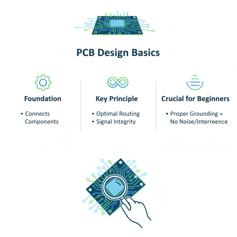
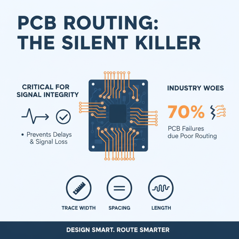
Understanding the basics of PCB design is crucial for anyone interested in electronics. A Printed Circuit Board (PCB) serves as a backbone for electronic devices. It connects components and supports their function. At its core, PCB design involves creating a layout that optimally routes electrical connections. Beginners often overlook the importance of grounding. Proper grounding is essential to avoid noise and interference.
For those with some experience, it's vital to focus on component placement. Cluttered layouts can lead to issues during assembly and debugging. Designers should also account for heat dissipation. Overheating components can fail prematurely, leading to costly mistakes. Integrating different layers of the PCB offers design flexibility. However, it can be challenging for novices and experts alike to manage complexity.
Many might forget to double-check their work. Design mistakes can be costly, especially in production. Inadequate testing leads to operational failures. Seeking feedback from peers can illuminate blind spots. Collaborative design reviews can highlight areas needing improvement. Embracing a mindset of learning helps in honing PCB design skills over time.
Essential Software and Tools for Effective PCB Design
When it comes to PCB design, having the right software and tools is essential. Many beginners often overlook this, which can lead to frustrating results. A reliable schematic capture tool can help visualize your circuit more clearly. This software allows you to create electrical diagrams easily. However, mastering such tools takes time and practice. Beginners must invest effort in learning their features.
Simulation tools are another vital component. They help verify designs before fabrication. Running simulations can save time and resources. Analyzing the results will point out potential flaws in your design. Experts often recommend using multiple simulation tools, as each has unique capabilities. Don't hesitate to experiment with them. It can lead to unexpected insights.
Additionally, consider using design rule checkers. These tools enforce standards within your PCB layout. Mistakes often occur here, especially in complex designs. Overlooking small details can lead to significant issues. Both novices and experts should regularly revisit their setups to refine their processes. This reflection can foster a deeper understanding of your design choice and lead to better outcomes.
Key Considerations for Schematic Layout and Component Placement
When designing a PCB, schematic layout and component placement play crucial roles. Start by keeping components organized and grouped by function. This approach can reduce the complexity of tracing connections. Additionally, consider the path of the power and ground lines. It’s essential to minimize interference and ensure good performance.
Placement is a balance of art and science. Place components close to where they are needed. This reduces the length of traces and minimizes potential noise issues. However, don’t forget about heat dissipation. Some components, like power regulators, generate heat. Allocate space around them for airflow.
It's also important to revise your layout regularly. Step back and evaluate your design. Are there areas that feel cluttered? Would a different arrangement improve performance? Learning from these reflections can significantly enhance future designs. Remember, every build offers lessons. Embrace the imperfection and grow from it.
Top 10 PCB Design Tips for Beginners and Experts
| Tip Number |
Design Tip |
Key Consideration |
Target Audience |
| 1 |
Start with a Schematic |
Ensure clarity in components and connections. |
Beginners |
| 2 |
Choose the Right Software |
Select tools that suit your project needs. |
All Levels |
| 3 |
Plan Component Placement |
Minimize trace lengths for better performance. |
Experts |
| 4 |
Use Ground Planes |
Improve signal integrity and reduce noise. |
All Levels |
| 5 |
Follow Design Rules |
Adhere to spacing and width requirements. |
Beginners |
| 6 |
Plan for Thermal Management |
Consider heat dissipation in placement. |
Experts |
| 7 |
Use Decoupling Capacitors |
Stabilize power supply quality near ICs. |
All Levels |
| 8 |
Run Design Rule Checks (DRC) |
Identify potential layout errors before production. |
All Levels |
| 9 |
Review and Iterate |
Continuous improvement leads to better designs. |
Experts |
| 10 |
Keep Learning |
Stay updated with the latest trends and technologies. |
All Levels |
Testing and Prototyping: Validating Your PCB Before Production
Testing and prototyping are crucial steps in PCB design. Before moving to production, validate your design. Each prototype reveals new insights. Errors can slip through. Small mistakes can lead to significant failures. For instance, trace widths might not support the necessary current. Conduct thermal tests to avoid overheating issues.
Using simulation software can enhance your prototyping process. It can identify electrical errors early. However, simulations may not catch all real-world scenarios. Always expect some level of discrepancy. Creating multiple prototypes helps refine your PCB. Each version teaches more about design limitations. Consider structural integrity under stress. Some parts may flex, affecting performance.
Don’t skip the testing phase. Poorly tested boards can lead to costly reworks. A PCB may look perfect, but functionality is key. Real-world testing gives a clearer picture. Share prototypes with peers for feedback. Fresh eyes can spot overlooked issues. Collaboration can lead to better designs and solutions.
Testing and Prototyping: Validating Your PCB Before Production