Choosing a PCB fab partner is not just a price exercise. A board that looks simple on a drawing can involve tight impedance control, fine-pitch features, and a delivery window measured in days. For global buyers, the real test is whether a supplier can repeat those results across prototypes and production runs.
Prismark’s 2024 industry review estimated global PCB production value at $73.6 billion, up 6.4% from 2023. That scale signals a competitive market, but it does not prove that every factory has the same process controls or regional support. IPC’s supply-chain research also points buyers toward visibility and resilience. IPC chief economist Shawn DuBravac has emphasized that supply-chain resilience depends on understanding risks and improving visibility; that principle matters when qualifying board suppliers, not just when placing orders. Check what each company can document: material traceability, inspection methods, engineering response times, and realistic capacity. Ask for evidence. A polished capability page is not an audit.
This Top 10 guide compares PCB fab companies for international sourcing, focusing on capabilities, certifications, service reach, and practical fit. The ranking is a starting point, not a universal verdict. A supplier that excels at high-volume multilayer boards may be a poor match for a fast-turn prototype. Some details remain difficult to compare from public information alone. Buyers should verify claims directly, request sample documentation, and assess communication before committing. In PCB sourcing, small gaps matter: a delayed clarification or unclear stack-up can cost more than a modest unit-price difference.

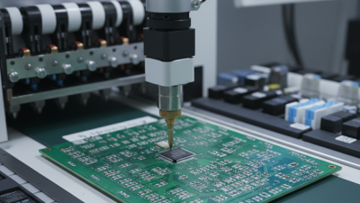
PCB fabrication companies turn engineering files into the physical circuit boards that connect components inside electronic products. Their work includes checking designs for manufacturability, selecting copper-clad materials, forming circuit patterns, drilling holes, plating connections, and inspecting finished boards. A small registration error can misalign a via; a weak plated barrel may fail after thermal cycling. Details matter.
The market is substantial. Prismark’s 2024 industry analysis estimated global PCB production value at about US$73.6 billion, reflecting demand across computing, communications, automotive, and industrial electronics. The World Semiconductor Trade Statistics organization reported global semiconductor sales of US$627.6 billion in 2024. Chips need reliable boards, and fabricators help translate rising component complexity into buildable products.
Not glamorous work. Buyers compare layer count, material capability, lead time, traceability, and test methods, not just quoted price. A capable supplier can flag tight tolerances before production and document inspection results for each lot.
Still, yield figures can conceal recurring rework, and published capability lists do not prove consistent execution. Buyers should review process controls, sample data, and communication practices.
One missed detail can cost weeks.

For an international PCB project, compare fabricators against the same drawing package, not just the quoted price. Include layer count, board thickness, copper weight, surface finish, and required impedance. Small differences matter. A 0.1 mm spacing change or a different laminate can affect manufacturability and signal performance. Ask each supplier to review the stackup and flag design-for-manufacturing risks before production. Clear questions reveal more than a polished capability list.
Check how quality is documented. Request current process certificates, inspection criteria, and a sample electrical test report. Confirm whether testing covers every board or a defined sample. Also ask how the supplier handles nonconforming panels and corrective actions. Compare lead times from design approval, not merely from order placement. For cross-border delivery, verify packaging, tracking, export documents, and who coordinates freight. Details can slip. I would not assume that the lowest quote includes the same inspection, materials, or shipping terms. One awkward point: supplier responses may be slower across time zones, even when the technical team is capable. Test communication with a real fabrication question, then assess how specifically the team answers. Requesting a small pilot build can expose gaps in yield, documentation, or packaging before larger quantities are committed.
A practical comparison framework using anonymous capability profiles. Specifications and schedules below are indicative industry ranges, not verified claims about individual suppliers.
| Profile | Typical project fit | Common layer range | Typical base materials | Indicative minimum trace / space | Indicative minimum finished hole | Common surface finishes | Typical prototype lead time* | International-buyer checks |
|---|---|---|---|---|---|---|---|---|
| 1. Rapid-turn prototype fabricator | Early electrical validation and engineering samples | 1–8 layers | FR-4; standard Tg options | About 5/5 mil (0.127/0.127 mm) | About 0.20 mm | HASL, lead-free HASL, ENIG | 3–7 working days | Confirm whether quoted time is fabrication time or delivered time; check shipping and customs estimates. |
| 2. Low-volume production fabricator | Pilot runs, product launches, and recurring small batches | 2–12 layers | FR-4; high-Tg FR-4 by request | About 4/4–5/5 mil | About 0.15–0.20 mm | HASL, ENIG, OSP, immersion silver | 5–10 working days | Compare setup charges, repeat-order pricing, panelization rules, and lot traceability. |
| 3. High-layer-count fabricator | Networking, computing, and complex control boards | 8–32+ layers, subject to design review | FR-4; high-Tg and low-loss laminates | About 3/3–4/4 mil on qualified designs | About 0.10–0.20 mm | ENIG, hard gold, OSP, immersion silver | 10–20+ working days | Request stack-up approval, impedance tolerances, registration capability, and a build-specific schedule. |
| 4. HDI fabricator | Compact devices using microvias and fine-pitch components | Typically 4–20+ layers | FR-4 and compatible HDI laminate systems | About 2.5/2.5–4/4 mil, design-dependent | Microvia dimensions and aspect ratios require design review | ENIG, ENEPIG, OSP | 10–25+ working days | Check sequential lamination, via-fill options, microvia reliability testing, and accepted drill files. |
| 5. Heavy-copper fabricator | Power conversion, energy systems, and high-current electronics | 1–12 layers | FR-4; thermal or high-Tg materials as required | Feature limits depend strongly on copper weight | About 0.20 mm or larger, depending on copper and stack-up | HASL, lead-free HASL, ENIG | 7–18 working days | Specify finished copper thickness, current requirements, thermal design, and allowable copper balance. |
| 6. RF and microwave fabricator | Radio-frequency, antenna, and high-frequency designs | 1–12 layers; hybrid stack-ups available at some facilities | Low-loss laminates, PTFE-based materials, and hybrid builds | Often about 3/3–5/5 mil; material and process dependent | Typically about 0.15–0.30 mm, design-dependent | ENIG, immersion silver, OSP | 10–25+ working days | Confirm exact laminate availability, dielectric data, controlled impedance, and material substitution policy. |
| 7. Rigid-flex fabricator | Space-constrained products requiring rigid and flexible sections | Commonly 2–12 total conductive layers | Polyimide flex materials with rigid-section laminates | Design-specific; flex geometry and copper type affect limits | Design-specific; drilled features must suit the stack-up | ENIG, ENEPIG, OSP, selective finishes | 15–30+ working days | Review bend radius, stiffeners, coverlay, copper grain direction, and mechanical drawing requirements. |
| 8. Metal-core and thermal-board fabricator | LED lighting and assemblies needing a heat-spreading base | Usually 1–2 conductive layers; specialized constructions vary | Aluminum-core; copper-core options may be available | Often about 5/5–8/8 mil, construction-dependent | Typically about 0.30 mm or larger | HASL, lead-free HASL, ENIG | 7–18 working days | Specify core thickness, dielectric thermal conductivity, breakdown voltage, and board flatness requirements. |
| 9. Automotive and high-reliability fabricator | Applications requiring documented process control and traceability | 2–20+ layers, depending on product and qualification | FR-4, high-Tg, and application-qualified materials | Capability is design- and qualification-dependent | Capability is design- and qualification-dependent | ENIG, OSP, immersion silver, selective finishes | Quote and qualification dependent | Request current certificates, change-control procedures, traceability scope, and product-specific qualification evidence. |
| 10. High-volume cost-focused fabricator | Stable designs with repeat production and cost-sensitive demand | Commonly 2–16 layers | Standard FR-4; approved alternatives by agreement | Often about 4/4–6/6 mil for mainstream builds | Often about 0.20–0.30 mm | HASL, lead-free HASL, OSP, ENIG | Production schedule varies by volume | Compare annual capacity allocation, tooling ownership, forecast terms, inspection plans, and approved-material controls. |
How to use this table: These profiles describe common fabricator specializations, not ranked or named companies. Actual limits depend on the complete stack-up, copper weight, board size, tolerances, inspection requirements, and factory process. Obtain a written design-for-manufacturing review and confirm certifications, export/shipping terms, lead time, and delivered cost for each specific project. *Lead times are indicative fabrication windows and generally exclude international transit, customs clearance, and design-review delays.
These ten profiles show different ways PCB fabricators serve global buyers. Profile 1 focuses on quick-turn prototypes, with small batches and close design feedback. Profile 2 handles high-volume boards, emphasizing repeatable processes and production planning. Profile 3 specializes in multilayer designs for compact electronics. Profile 4 offers flexible order sizes for early-stage product teams. Profile 5 supports rigid-flex boards, where careful bend-radius checks matter. Each model has trade-offs.
Profile 6 serves buyers seeking heavy-copper boards for demanding power applications. Profile 7 concentrates on high-frequency materials and controlled impedance. Profile 8 combines fabrication with assembly coordination, which can simplify handoffs. Profile 9 focuses on tight tolerances and detailed inspection records. Profile 10 supports varied board types, though broad capability does not always mean equal strength in every process. Ask for evidence, not just claims. A polished website proves little.
Tips: Send the same files and requirements to each candidate. Compare stack-up proposals, minimum feature limits, lead times, and inspection reports. Ask how they handle a drill shift or a failed coupon test. Check whether quoted tolerances match your drawing. Start with a representative sample when feasible. One thing is easy to overlook: communication during a problem can reveal more than a sales call.
Nominal copper thickness by common copper-foil weight. Use this reference when comparing PCB fabrication specifications; actual finished copper thickness may vary by process.
Copper weight is expressed in ounces per square foot. The chart uses the approximate conversion 1 oz/ft² = 34.8 μm.
A PCB fabricator’s capabilities should match the board, not just the buyer’s target price. Ask whether it handles your layer count, material type, copper weight, and minimum trace spacing. Request sample cross-sections and inspection records for comparable work. A production-ready process may include controlled impedance testing, electrical testing, and documented inspection criteria. Details matter. A board with dense routing can expose limits that a simple prototype never reveals.
Certifications help buyers assess quality systems, but their scope deserves a close look. ISO 9001 covers quality management; sector-specific standards may apply to automotive or medical work. Confirm that the certificate is current and covers the actual production site and process. A tidy certificate folder is not proof of consistent output. Ask how nonconforming boards are contained, investigated, and reported. The answer should be specific, not rehearsed.
Delivery networks shape the real lead time. Check where boards are fabricated, where they ship from, and how customs paperwork and tracking are handled. For urgent builds, ask about capacity reservation and realistic dispatch dates, not only advertised turnaround. Regional warehousing can reduce transit time, though it may add handling steps. One detail buyers sometimes overlook: holidays and local cut-off times can shift a shipment by days. Plan for that, and leave room for an imperfect forecast.
Choosing a PCB fabrication partner starts with the board, not the sales pitch. Share your layer count, material, copper weight, finished thickness, and target quantity. A clear specification helps suppliers quote comparable work. Ask whether they can meet your required line widths, spacing, and tolerances, then request sample inspection records. Details matter.
Production capability is only part of the decision. Check how quickly the engineering team answers questions about drill files, stack-ups, or panelization. A useful partner flags unclear data before production rather than guessing. Ask about test methods, defect handling, and how revisions are tracked. For a first order, a small pilot batch can reveal whether the boards match the drawings and arrive in suitable packaging. It also tests communication under real deadlines.
Global delivery adds practical risks. Confirm the shipping method, export paperwork, packaging protection, and the person responsible for resolving delays. Compare total landed cost, not just the quoted board price. Be cautious of unusually low bids with vague inspection details. Still, no checklist removes every risk; even a careful review can miss a process weakness. That is why references, written specifications, and a defined response plan matter.