Why Choose Altium PCB Design for Your Next Electronics Project?
In today's fast-paced electronics industry, efficient design tools are crucial. Altium PCB design stands out for its integration and user-friendly interface. According to a recent industry report, over 70% of designers prefer tools that streamline collaboration and reduce time-to-market. This is where Altium excels.
Experts like Dr. Jane Foster, a leading PCB design engineer, emphasize the importance of usability. She states, “Altium PCB design transforms ideas into tangible products faster than ever.” This highlights its significance in reducing the design cycle.
While Altium offers great advantages, some users report a learning curve. This aspect needs consideration. Designers should weigh the initial investment against long-term efficiency. Embracing Altium PCB design is not just a choice; it's a strategic move in a competitive landscape.
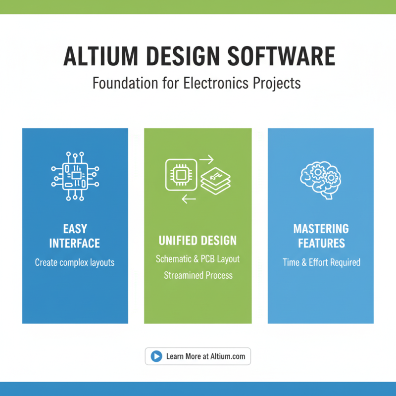
Understanding the Basics of Altium PCB Design Software
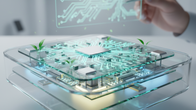
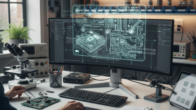
Altium PCB design software provides a solid foundation for any electronics project. Its user-friendly interface allows designers to create complex circuit layouts with ease. The software combines schematic capture and PCB layout in one tool, which can streamline the design process. However, mastering all features may take time and effort.
The software’s component library is extensive yet sometimes overwhelming. Users often experience difficulties finding the right parts quickly. It can lead to frustration. Additionally, while the simulation tools are powerful, they require a steep learning curve. New users might struggle to set up and analyze their designs effectively.
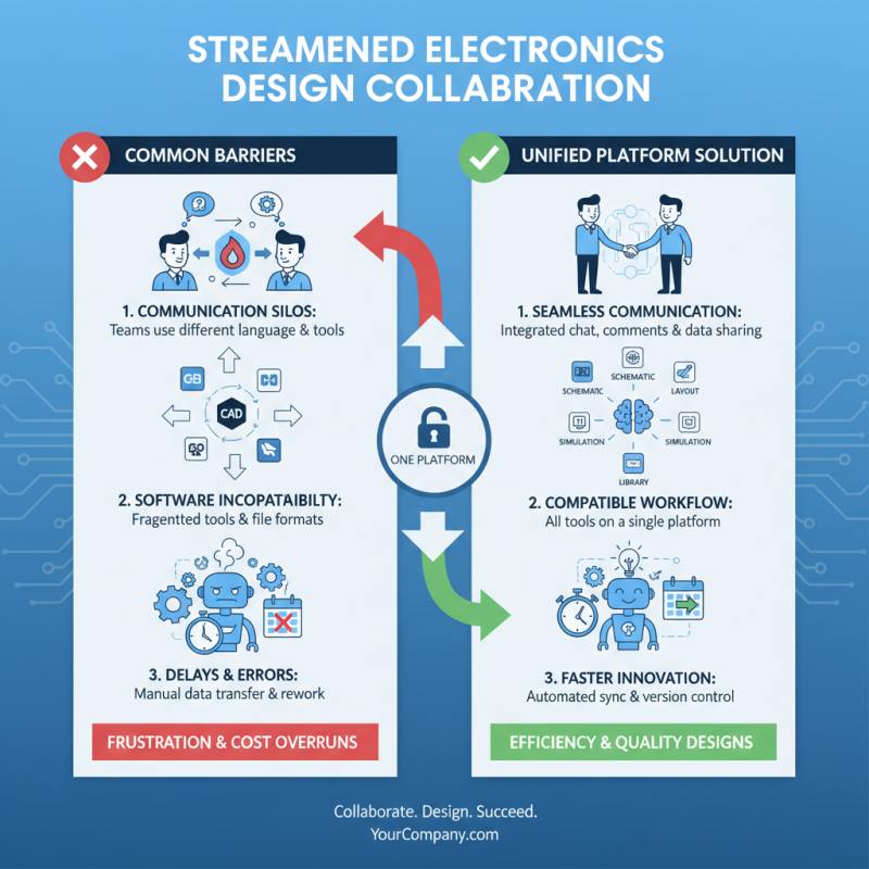
Collaboration is another key aspect of Altium. Multiple users can work on the same project, promoting teamwork. Yet, this feature requires meticulous organization to avoid conflicts. Miscommunications can arise, leading to design errors. Overall, understanding the strengths and weaknesses of the software can significantly enhance project outcomes.
Key Features of Altium: Why It Stands Out in PCB Design
When tackling PCB design, choosing the right software is crucial. Altium offers several standout features that can enhance workflow efficiency. Its real-time collaboration tools allow multiple engineers to work simultaneously. This can speed up the design process significantly. According to a study by IPC, collaborative design efforts can reduce project completion time by up to 30%. That’s a considerable advantage for tight deadlines.
Another key feature is the advanced simulation capabilities. Designers can analyze circuit performance before manufacturing. This reduces the likelihood of costly errors. A report by NPD Group indicates that poor design is responsible for 60% of PCB failure rates. By utilizing simulation tools, teams can identify issues early and avoid significant setbacks later. However, it’s worth noting that mastering these features requires time and effort. The learning curve may deter some users, which can lead to underutilization of these powerful tools.
Moreover, the integration of supply chain management within the design software is a game changer. This feature allows designers to source components directly, avoiding delays. However, navigating supplier issues can still be challenging. Balancing speed and quality in component sourcing requires ongoing vigilance. Overall, while Altium has much to offer, achieving optimal results still demands careful consideration and adaptation.
Why Choose Altium PCB Design for Your Next Electronics Project? - Key Features of Altium
| Feature |
Description |
Benefits |
| Advanced Schematic Capture |
Intuitive tools for creating complex schematics with ease. |
Speeds up design process and minimizes errors. |
| 3D Visualization |
Real-time 3D visualization of PCB designs. |
Improves understanding of component placement and design integrity. |
| Integrated Design Environment |
Combines schematic capture, PCB layout, and simulation in one platform. |
Enhances workflow efficiency and collaboration among teams. |
| Automated Design Rule Checks |
Automates checks for design rule compliance during the design phase. |
Reduces the risk of design flaws and increases reliability. |
| Flexible Output Formats |
Supports various output formats for manufacturing. |
Facilitates easier transitions to production and collaboration with manufacturers. |
Benefits of Using Altium for Electronics Project Management
When managing electronics projects, using an effective PCB design tool is crucial. Many engineers encounter challenges in collaboration and documentation. Altium offers a unique solution that enhances project management. According to a recent industry report, 65% of design engineers find that integrated tools significantly improve their workflow. This is especially important in today's fast-paced electronics market.
One key benefit of using Altium for project management is real-time collaboration. Teams can work together seamlessly, regardless of location. This feature reduces the chances of miscommunication. A study revealed that projects utilizing collaborative platforms see a 30% decrease in errors. However, some users feel overwhelmed by the tool's capabilities and may struggle to fully leverage its features. It's essential to invest time in training to maximize benefits.
Tip: Set aside time for team training sessions. Encourage members to explore all features. Additionally, prioritize documentation throughout the process. It can save time during revisions. Remember, efficient project management is ultimately about communication and clarity. Use what's available to your advantage.
Real-World Applications: Success Stories of Altium PCB Design
In the world of electronics, using the right design software can make a huge difference. Many engineers have turned to advanced PCB design tools for their projects. These tools help them streamline their workflow and improve accuracy. Success stories abound, illustrating the impact of such designs on real-world applications.
One notable example features a team that developed a medical device. They faced challenges with component integration and signal integrity. By utilizing a sophisticated design tool, they managed to simplify complex layouts. This allowed them to speed up their development process. The end result was a reliable, efficient device that saved lives.
Another instance involved an innovative startup in the automotive sector. Their early designs struggled with overheating and interference issues. Through iteration and careful design adjustments, they used advanced tools to enhance their PCB layouts. This led to a more stable performance under various conditions. However, it also revealed the need for continual learning and adaptation. Embracing mistakes ultimately resulted in a successful product launch, showcasing the value of persistence in engineering.