What Is Circuit Board Assembly and How Does It Work?
Circuit board assembly is where an engineered design becomes a working electronic product. Bare boards, components, solder paste, and inspection systems meet on a controlled production line. A tiny resistor may be placed beside a high-speed processor, while automated optical inspection checks every visible solder joint. The process looks mechanical. It is not entirely predictable.
The market explains its importance. Fortune Business Insights valued the global printed circuit board market at approximately US$83.25 billion in 2024. Its report forecasts continued growth through 2032, driven by automotive electronics, telecommunications, medical devices, and consumer technology. The IPC Global Electronics Manufacturing Supply Chain Outlook also emphasizes persistent pressure on materials, capacity, quality, and delivery performance. These pressures affect circuit board assembly directly. One misplaced component can delay testing, shipping, and customer acceptance.
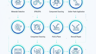
Hayao Nakahara, a respected PCB industry analyst, famously described the printed circuit board as “the mother of all electronics.” His observation remains practical. Assembly determines whether that foundation performs reliably inside a real product. The workflow usually includes solder-paste printing, component placement, reflow soldering, inspection, and functional testing. Through-hole assembly may follow for larger connectors or mechanical parts. Details matter.
A clean stencil is not enough. Moisture, heat profiles, component tolerances, and operator decisions can still create defects. That is the uncomfortable part. Reports provide direction, but factory evidence provides confidence. This guide examines how circuit board assembly works, why each stage matters, and where quality problems quietly begin.
Defining Circuit Board Assembly and Its Role in Electronics
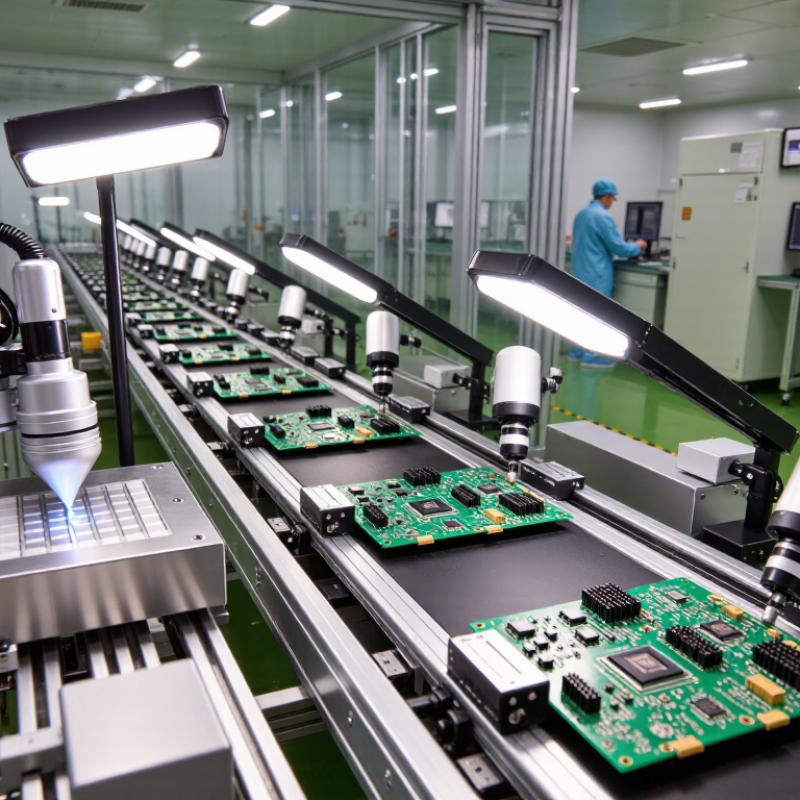
Circuit board assembly is the process of attaching electronic components to a printed circuit board. It turns a bare board into a working electronic unit. Components may include resistors, capacitors, processors, connectors, and sensors. Assembly usually begins with applying solder paste to precise contact points. A placement machine then positions components on the board. Heat melts the paste and creates lasting electrical connections.
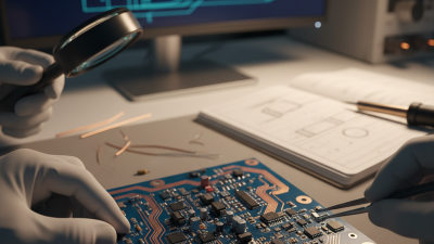
Its role in electronics is both practical and critical. Assembly connects the circuit design with real hardware, allowing signals and power to move correctly. Quality depends on accurate placement, controlled heating, clean surfaces, and careful inspection. Technicians may use optical inspection, electrical testing, and visual checks under magnification. A small solder bridge can stop an entire device from working. A missing component can create similar trouble. Assembly is not merely a production step. It strongly affects reliability, repair costs, and product safety. Still, a perfect first pass is not guaranteed. Even experienced teams can overlook subtle defects.
Tips: Keep component lists and assembly drawings updated. Confirm polarity before soldering. Inspect fine-pitch areas closely. Record test results for traceability. If a board fails, review the process rather than blaming one component immediately. Sometimes the real issue is a temperature change, a worn stencil, or an unclear instruction.
Key Components and Materials Used in Board Assembly
Circuit board assembly turns a bare circuit board into a working electronic unit. The process starts with a substrate, usually fiberglass-reinforced epoxy, carrying copper traces. Solder pads connect components through carefully designed conductive paths. Resistors control current, capacitors store and release charge, and integrated circuits perform programmed functions. Connectors provide external access, while diodes protect circuits from unwanted current. Each part has a footprint, tolerance, and temperature rating that must match the design.
During assembly, solder paste is applied through a stencil onto the pads. A placement machine positions tiny components, sometimes smaller than a grain of rice. Controlled heating melts the paste and forms solder joints. Larger or through-hole parts may need selective soldering or careful hand placement. Technicians inspect alignment, polarity, and joint shape through visual checks and automated inspection. A board can look perfect and still fail. Electrical testing is therefore essential, although test coverage is never absolute. That limitation deserves honest attention.
Tips:
Keep moisture-sensitive materials sealed until use, and record storage time. Verify component references before placement, especially for polarized parts. Use clean tools and controlled handling to reduce contamination. Check solder joint samples under magnification. Do not treat inspection as proof of reliability; temperature cycling and functional tests can reveal weaknesses that a quick visual check misses. Good assembly depends on material quality, process control, and disciplined records.
How Components Are Placed and Soldered onto a Circuit Board
Circuit board assembly turns a bare PCB into a functional electronic unit. Component placement begins with design files, feeder setup, and a controlled solder paste pattern. A stencil printer spreads paste across copper pads. An automated placement machine then picks resistors, capacitors, and integrated circuits. It places each part against programmed coordinates. Tiny misalignment matters. Fine-pitch packages leave little room for error.
The board then enters a reflow oven, where a carefully controlled temperature profile melts the paste. The solder cools into solid joints around each component lead. Through-hole parts require drilled holes and may use selective soldering. Technicians inspect the assembly with automated optical inspection, X-ray imaging, and electrical testing. IPC-A-610 and J-STD-001 provide widely used acceptance and soldering criteria. The WSTS Spring 2024 Forecast expected global semiconductor sales to reach 611.2 billion dollars in 2024, increasing pressure on assembly quality and capacity.
Inspection is not merely a final gate. It also reveals weak stencil cleaning, lifted leads, and uneven heating. A clean-looking joint can still hide a void underneath. That is why experienced teams compare inspection images with oven profiles and placement data. Production numbers can look impressive while defects remain unnoticed. Data needs context. Human review still matters. Errors happen. Even well-tuned lines need regular calibration, process checks, and honest questioning of their assumptions.
Common Assembly Technologies and Their Practical Applications
What Is Circuit Board Assembly and How Does It Work?
Circuit board assembly turns bare boards into tested electronic hardware. The dominant approach is surface-mount technology, or SMT. Machines place tiny components onto solder paste, then a reflow oven melts the connections. This supports dense designs in phones, industrial controllers, medical monitors, and vehicle modules. A 2024 analysis from Grand View Research valued the global PCB market at about US$89 billion in 2023. That figure covers more than assembly, so it needs careful interpretation.
Through-hole technology, or THT, remains practical for large connectors, transformers, and stress-bearing components. Mixed technology combines SMT density with THT strength on one board. Selective soldering heats chosen joints, reducing thermal exposure and rework. Automated optical inspection checks placement and solder shape. X-ray inspection finds hidden defects beneath components. Mordor Intelligence’s 2024 PCB assembly analysis identifies SMT as the leading process segment. However, production volume does not guarantee reliability. Moisture, pad design, and operator setup still matter.
Tips: Match technology to stress, size, and production volume. Request first-article inspection records and traceable test results. IPC workmanship criteria help define acceptable solder joints. Build a prototype before scaling. It costs more early. It may prevent expensive rework later.
PCB Assembly Technologies: Typical Package Pitch
Smaller pitch supports higher component density but generally requires tighter process control, accurate placement, and advanced inspection.
Through-hole assembly commonly uses 2.54 mm connector spacing and is well suited to mechanically robust interfaces and high-power parts. Surface-mount packages such as SOIC, QFP, and BGA enable more compact circuit boards. The pitch values shown are representative industry-standard package dimensions; actual values vary by component series and design requirements.