Top PCB Design Course Essentials for Aspiring Electronic Engineers?
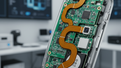
In today's fast-evolving electronics industry, mastering a PCB design course is crucial for aspiring engineers. This training not only covers the fundamentals of circuit design but also delves into advanced techniques. Students learn to create intricate layouts and understand material selection.
Effective PCB design requires both theoretical knowledge and practical skills. It's a challenge to balance creativity with functionality. Mistakes are inevitable, and students often struggle with initial designs. However, these setbacks can catalyze growth and innovation. Each error presents a learning opportunity that shapes a more competent engineer.
The right PCB design course should offer hands-on projects. Real-world applications enhance understanding and retention. Aspiring engineers should seek programs that encourage experimentation. As they navigate through complex problems, their confidence and problem-solving abilities will grow. Embracing imperfections leads to better designs.

Essential PCB Design Principles for Beginners in Electronic Engineering
PCB design is a crucial skill in electronic engineering. Beginners must grasp essential principles to create effective and reliable circuit boards. According to a report by IPC, the global PCB market was valued at over $60 billion in 2021, highlighting the industry's growth. Understanding the fundamentals can lead to innovative designs and career opportunities.
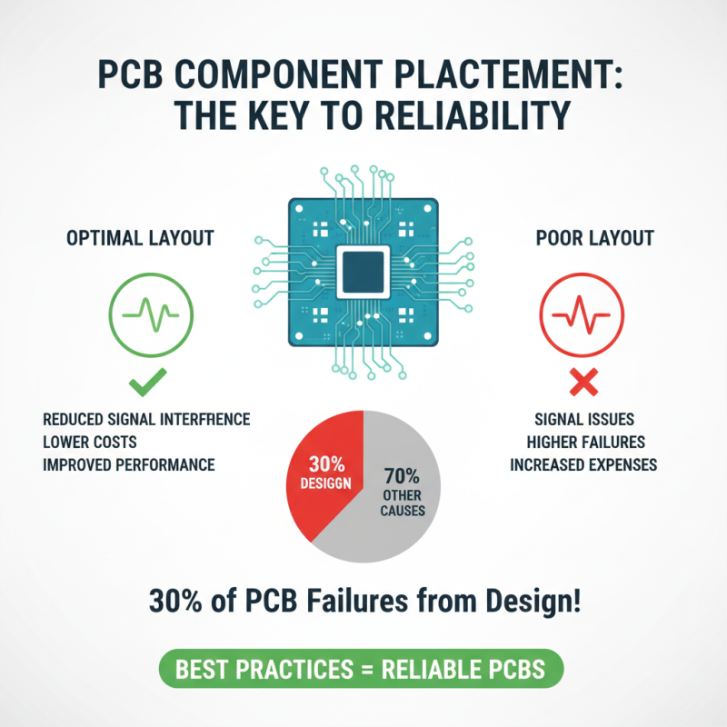
One key principle is layout optimization. This involves placing components for minimal interference and maximum performance. Poor layouts can cause signal integrity issues. In fact, nearly 30% of PCB-related problems arise from insufficient component placement. Learning to utilize simulation tools can help engineers visualize potential issues early in the design phase.
Another critical aspect is material selection. Different applications require specific materials. For example, high-frequency circuits often need low-loss substrates. A study published by the IEEE indicates that 40% of PCB failures stem from inappropriate material choices. New designers should familiarize themselves with different types of materials, and their trade-offs, to avoid costly mistakes.
Understanding PCB Materials and Their Impact on Circuit Performance
When designing printed circuit boards (PCBs), material choice is crucial. PCB materials, like FR-4 and CEM-1, affect performance. The dielectric properties of these materials influence signal integrity. For high-frequency applications, loss tangent matters. Low loss tangent materials can drastically improve signal transmission.
Thermal management is another key factor. Different materials dissipate heat differently. Some designs might overheat due to inadequate heat sinking. This can lead to circuit failure. Reflecting on past failures helps in understanding material limits. It’s essential to test prototypes thoroughly under various conditions.
Moreover, cost often influences material selection. Cheaper materials can compromise performance. Engineers may think short-term savings are viable. However, this can lead to long-term issues. Balancing budget with performance is challenging yet necessary. Understanding these aspects is vital for success in PCB design.
Top PCB Design Course Essentials for Aspiring Electronic Engineers
| Material Type |
Dielectric Constant (Dk) |
Loss Tangent (Df) |
Thermal Conductivity (W/m·K) |
Common Applications |
| FR-4 |
4.2 |
0.02 |
0.3 |
Consumer Electronics, General Purpose |
| Polyimide |
3.2 |
0.01 |
0.25 |
Aerospace, High-Temperature Applications |
| PTFE (Teflon) |
2.1 |
0.001 |
0.2 |
High-Frequency Applications, RF Circuits |
| CEM-1 |
5.0 |
0.03 |
0.15 |
Low-Cost Boards, less critical applications |
Key Software Tools for PCB Design: A Comprehensive Overview
When diving into PCB design, understanding essential software tools is crucial. Various platforms offer unique features. Some focus on user-friendly interfaces, while others prioritize advanced functionalities. Electronic engineers should grasp these nuances.
Familiarity with schematic capture is vital. This allows engineers to create circuit diagrams easily. Simulation software complements this by testing circuit behavior before production. However, not all simulations provide accurate results. Users must critically evaluate their tools and adjust designs as needed.
Layout tools are equally important. They help translate schematics into physical designs. However, learning these tools can be daunting. Engineers often face challenges in component placement and routing. It’s essential to practice regularly and seek feedback to improve skills.
Best Practices for PCB Layout and Component Placement Techniques
When designing a PCB, placement is key. Poor layout can lead to signal interference and increased costs. According to industry reports, nearly 30% of PCB failures stem from design errors. This emphasizes the importance of best practices in component placement.
Optimizing the layout can improve performance significantly. Placing high-frequency components close to each other reduces noise. Moreover, adhering to proper spacing guidelines prevents thermal issues. Yet, not all engineers follow these protocols. Inexperience can result in mistakes that could have been avoided. For every 100 boards manufactured, about 15% may need redesign due to placement errors.
Additionally, understanding the power distribution is crucial. A well-planned power plane minimizes voltage drop and enhances current flow. Yet, many designers overlook this aspect. The placement of decoupling capacitors near power pins is often neglected. Failing to consider these factors can lead to inefficiencies. Engineers must continuously reflect on their designs for improvements.
Troubleshooting Common PCB Design Issues in Electronic Engineering
When designing PCBs, troubleshooting common issues is essential. Poor connections can lead to malfunctions. A joint may appear fine but still cause problems. Always double-check solder joints to ensure they are secure. Visual inspections can reveal cracks or cold solder joints.
Another frequent issue is signal interference. Long traces can pick up noise, impacting performance. Keep traces short and use ground planes to minimize this risk. Experimenting with trace widths and spacing can also help. The layout must prioritize signal integrity.
Lastly, managing thermal issues is critical. Components can overheat if not properly spaced. Ensure adequate ventilation and consider heat sinks if necessary. If overheating still occurs, reassess the design. Review component placements and recalibrate parameters. Trial and error plays a huge role in PCB design.
Top PCB Design Course Essentials for Aspiring Electronic Engineers