Top 5 PCB Software Tips for Efficient Design and Manufacturing?
In the ever-evolving world of electronics, efficient PCB design is crucial. Renowned PCB software expert Dr. Emily Chen emphasizes, "The right PCB software can save time and reduce errors." This insight captures the essence of effective design and manufacturing.
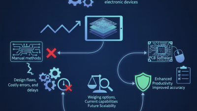
When navigating PCB software, understanding its features is paramount. Many designers overlook essential tools that streamline the workflow. Efficiency is more than a buzzword; it's about maximizing resources. Clarity and precision in layouts can significantly impact product performance.
Nonetheless, even experienced designers face challenges. The learning curve of advanced PCB software can be steep. Mistakes can arise from overlooking a single setting. Reflecting on these points reveals that continuous learning and adaptation are vital in this field.
Top PCB Software Features to Enhance Design Efficiency
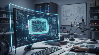
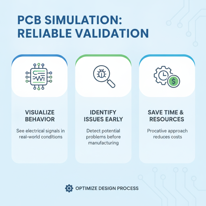
When selecting PCB software, efficiency is key. Many tools offer features that enhance design workflow. One important feature is real-time design rule checking. This functionality quickly identifies errors, preventing costly mistakes later in the manufacturing process. Effective PCB design software should also include advanced simulation capabilities. These allow designers to test their circuits virtually, saving time and resources.
Another essential feature is a user-friendly interface. A clean layout can significantly reduce the learning curve for new users. While some software may promise advanced capabilities, usability can make a difference in daily tasks. This highlights the need for balance. Complex tools can overwhelm, hindering rather than helping the design process.
Collaboration tools are also critical in PCB design. Effective software should allow multiple users to contribute seamlessly. However, while these tools can promote teamwork, they can also introduce confusion if not managed properly. Keeping track of changes is vital for maintaining the integrity of the design. Investing time in learning these features can enhance overall efficiency, leading to better design outcomes.
Understanding Layer Stackup: Crucial for Optimal PCB Design
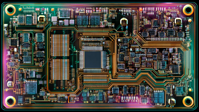
Understanding layer stackup in PCB design is fundamental for achieving efficiency in both design and manufacturing. The layer stackup refers to the arrangement of copper, dielectric, and other materials in a PCB. A well-thought-out stackup can markedly improve signal integrity, thermal management, and overall reliability. Designers must consider impedance control and electromagnetic interference when defining the stack layers.
Choosing the right materials for each layer is essential. Different substrates have varying properties that influence performance. For instance, high-frequency applications might necessitate specific materials to reduce losses. Yet, many designers overlook material selection, impacting finished product performance. Reflecting on past projects can help uncover these oversights.
Additionally, the number of layers should be carefully determined. Adding layers increases complexity and cost. It’s crucial to balance the need for additional layers with practicality. Many times, simpler designs yield better results. Analyzing previous designs can offer insights into optimizing stackup, ensuring a more efficient manufacturing process.
Importance of Design Rule Check (DRC) in Manufacturing Precision
Design Rule Check (DRC) is vital in PCB manufacturing. It ensures that your designs comply with specific standards. These standards help in avoiding common pitfalls that can lead to costly errors. When DRC is implemented effectively, it reduces the risk of production delays and enhances overall reliability.
Common DRC errors include clearance violations and trace width discrepancies. Such issues can compromise the functionality of the final product. It's essential to invest time in setting appropriate design rules. Regularly review your settings, as they may require adjustments based on varying project requirements. Neglecting DRC could lead to significant setbacks in the production process.
Moreover, DRC helps in maintaining a consistent quality across different batches. This consistency is crucial for long-term projects, where reliability is key. However, not all software tools are user-friendly. Some may provide inaccurate feedback, leading designers astray. Continuous learning and familiarity with DRC features can mitigate these challenges, ensuring a smoother design experience.
Top 5 PCB Software Tips for Efficient Design and Manufacturing
Integrating Collaboration Tools for Streamlined Team Workflows
Effective collaboration is crucial in PCB design and manufacturing. Integrating collaboration tools can significantly enhance team workflows. These tools facilitate real-time communication among engineers, designers, and project managers. When everyone is on the same page, the chances of miscommunication decrease.
Creating a shared platform for document management is essential. It allows team members to access the latest design files and updates easily. Regular updates in these documents are vital to prevent errors. Relying solely on traditional emails often leads to confusion and delays. Teams benefit from using visual management tools to track progress and assign tasks.
However, not all collaboration tools suit every team. Each team has unique needs and preferences. Finding the right balance can take time. Assessment of which tools enhance productivity the most helps refine workflows. Continuous feedback loops should be part of the process, allowing for adjustments when needed. Embracing collaboration is a journey toward more efficient PCB design.