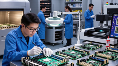
Why Choose PCB Manufacturing and Assembly Services?
Choosing pcb manufacturing and assembly services can turn a promising design into a dependable, testable product. The right partner reviews more than board dimensions. It checks material choices, copper weight, trace spacing, component availability, and assembly requirements before production begins. Small details matter. A misplaced connector or an unsuitable solder mask can create delays, rework, or field failures.
PCB design educator Rick Hartley is often associated with the reminder, “A PCB is a component.” That idea captures why fabrication and assembly should be considered together, not treated as separate purchasing tasks. When engineers and manufacturers review the design early, they can identify risks such as difficult-to-source parts, tight tolerances, or a layout that complicates inspection. The result may be a smoother path from prototype to repeatable production, though no supplier can remove every risk.
A capable service provider can also offer engineering feedback, controlled assembly processes, and documented testing. Ask how it handles design-for-manufacturing reviews, component substitutions, inspection, and traceability. Request clear answers, not broad promises. Even a strong supplier can miss a detail; that possibility deserves honest review. Compare actual capabilities against your product’s needs, including order volume, delivery schedule, and quality expectations. Done carefully, pcb manufacturing and assembly services can reduce coordination work and help teams make better-informed production decisions.
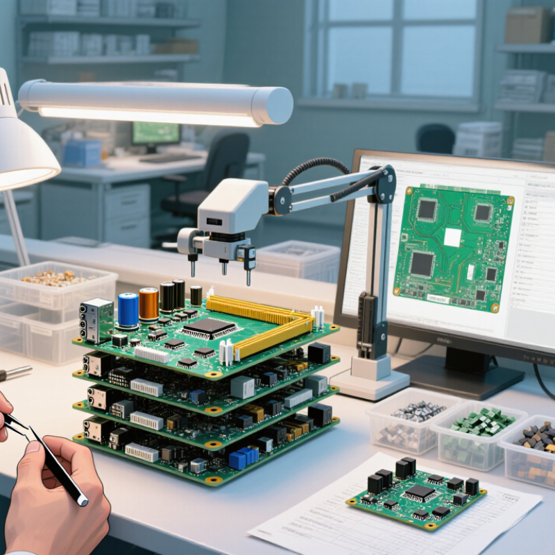
What PCB Manufacturing and Assembly Services Include
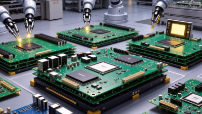
PCB manufacturing and assembly services turn a circuit design into a tested, populated board. The process often starts with a design-for-manufacturing review. Engineers check trace spacing, hole sizes, layer stack-up, and component clearances before production. Small errors here can cause costly delays later.
Fabrication may include copper-layer imaging, etching, drilling, plating, solder-mask coating, and silkscreen printing. Boards are then electrically tested for opens and shorts.
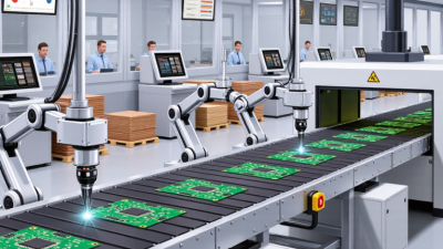
Assembly adds components using surface-mount or through-hole methods. Typical steps include solder-paste printing, automated placement, reflow soldering, and inspection. A populated board may also receive X-ray checks, programming, and functional testing, depending on its components and intended use.
Not every board needs every check. The right test plan depends on design risk and production volume.
Grand View Research estimated the global PCB market at USD 76.12 billion in 2023, reflecting the scale of demand for reliable board production. That figure does not mean every project needs the same service package.
A clear bill of materials, accurate assembly files, and agreed inspection criteria help prevent avoidable rework. Missing details still happen. A connector orientation, for example, can be easy to overlook.
How PCB Designs Become Assembled Circuit Boards
Turning a PCB design into an assembled circuit board takes a sequence of precise, connected steps. Manufacturing files, drill data, and a parts list describe what the fabricator needs to build. Engineers review clearances, copper thickness, hole sizes, and component footprints before production. This review matters. A footprint can look correct on screen yet leave a connector tilted or its pads poorly wetted. Small errors hide well.
The bare board is formed from layered material and patterned copper. Holes are drilled, surfaces are finished, and solder mask protects areas that should not conduct. After inspection, solder paste is applied through a stencil onto component pads. Automated placement sets tiny parts onto the paste, then controlled heat melts it into electrical and mechanical joints. Larger parts may need hand placement or a separate through-hole soldering step. The board is then checked for missing parts, shifted components, and solder bridges. Optical inspection helps, but it cannot confirm every electrical function. Depending on the design, continuity checks or a powered functional test may be needed. No checklist catches every issue, so clear assembly notes and realistic testing plans matter. A design that assembles cleanly is not always perfect; sometimes the first build reveals a spacing or access problem worth correcting.
Why Combining Fabrication and Assembly Matters
Choosing one provider for board fabrication and assembly can reduce handoffs between design and production teams. The same engineering group can review copper layers, drill data, solder-mask openings, and component placement together. That alignment matters. A plated hole positioned too close to a component may pass fabrication checks but complicate soldering. When fabricators and assemblers share feedback early, they can flag clearance, panelization, or stencil concerns before boards are built. Small details matter.
Assembly feedback can also improve the next board revision, especially when technicians record recurring defects such as lifted pads or uneven solder joints. The team can compare inspection findings with the original design files, rather than relying on assumptions or scattered emails. This does not remove every risk. A combined service may shorten communication loops, but it cannot guarantee lower cost or flawless output. A buyer should still ask how design changes are approved, how materials are tracked, and what inspection records are supplied. Some projects may benefit from separate specialists; coordination can still miss issues if responsibilities remain vague.
Benefits for Quality, Cost, and Production Speed
PCB manufacturing and assembly services bring fabrication, component sourcing, and board population into one coordinated workflow. That can reduce handoffs, where specifications sometimes get lost. IPC-A-610 and J-STD-001 provide widely used criteria for assembled-board acceptability and soldering. Automated optical inspection can flag misaligned components or solder defects, while X-ray inspection helps examine hidden joints. These tools improve visibility, but they do not make quality automatic. A poorly reviewed design can still create repeat defects.
Bringing production steps together can also help control cost and lead time. NIST’s FY2023 Manufacturing Extension Partnership impact data reported $1.4 billion in cost savings among manufacturers it assisted. This is an aggregate figure, not a PCB-specific result, but it shows how process improvements can matter financially. In practice, early design-for-manufacturing checks may catch issues such as tight component spacing before boards reach the line. That is often cheaper than reworking assembled boards. Faster, too. Yet quick production depends on parts being available and design files being stable. A late component change can undo days of schedule gains. The less glamorous work—clear documentation, test planning, and careful revision control—often protects both quality and delivery speed.
Why Choose PCB Manufacturing and Assembly Services?
Indicative production planning ranges for a PCB order (business days)
Using one manufacturing and assembly partner can simplify coordination across fabrication, sourcing, assembly, and testing. These indicative ranges vary with board complexity, component availability, order quantity, and inspection requirements. Request a project-specific quote for accurate timing and cost.
How to Choose a PCB Service Provider
A capable PCB service provider should understand your design, production volume, and assembly needs before quoting. Share your Gerber files, bill of materials, and expected order quantity. Ask whether engineers review clearances, drill sizes, and component footprints before fabrication. That review can catch costly mismatches early. Ask for evidence. Request sample inspection records or a clear explanation of electrical testing and inspection options. Details matter.
Compare providers on more than price. Check their capabilities for board materials, layer counts, surface finishes, and component sourcing. Confirm how they handle parts that are unavailable or substituted; changes should be approved before assembly. Ask about production updates, packaging, and how defects are documented. A fast response is useful, but a specific answer about your board is more telling. It is easy to overvalue a polished quote. Recheck the assumptions behind it, especially lead time and test coverage.
Tips: Send complete, current files and mark critical dimensions clearly. Request a small prototype run when practical, then inspect solder joints, connector fit, and board dimensions. Keep communication in writing. If a provider’s process is not clear, ask again before committing.