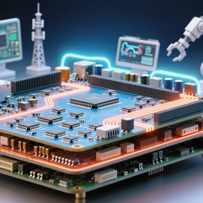
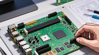
PCB board design is the quiet discipline behind reliable electronic products. It determines how power, signals, heat, components, and manufacturing constraints work together. A trace is not merely a line on a screen. It has impedance, resistance, a return path, and physical consequences.
Market evidence shows why this work matters. Fortune Business Insights valued the global PCB market at approximately USD 81.74 billion in 2023. Its 2024 report projects continued growth through 2032, driven by automotive electronics, telecommunications, industrial automation, and connected devices. IPC’s PCB industry reports also highlight ongoing pressure around supply capacity, material costs, quality, and delivery performance. These pressures make design decisions commercially important, not only technically interesting.
Rick Hartley, a respected PCB design and signal-integrity educator, often emphasizes, “The return path is as important as the signal path.” That principle appears on the workbench quickly. A fast digital trace may look correct in CAD, yet create noise when its reference plane is interrupted. A copper pour may seem helpful, but it can complicate thermal balance or assembly access. Small choices matter.
Good pcb board design connects engineering intent with production reality. It considers IPC-2221 guidance, IPC-6012 performance requirements, component tolerances, stack-up planning, and design-for-manufacturing checks. Still, no checklist guarantees perfection. A polished layout can fail testing. That uncomfortable possibility deserves attention. The strongest process reviews assumptions early, measures critical behavior, and leaves room for correction before fabrication begins.
PCB board design means deciding how a circuit will be arranged, connected, powered, and manufactured. It controls more than the visible copper traces. It also influences signal quality, heat movement, mechanical fit, testing, and long-term reliability.
In practice, designers place components according to function and current flow. A processor may need short connections to memory, while a power section needs wider copper paths. Ground planes provide controlled return paths and can reduce unwanted noise. Small vias connect different layers, but too many can complicate manufacturing. Even a connector’s position matters when cables must bend inside a tight enclosure.
PCB design also controls how confidently a board can be built and repaired. Clearances, hole sizes, soldering areas, and test points affect production results. A layout may work in simulation yet fail when heat rises or a fast signal crosses a noisy power region. That gap requires physical testing, measurement, and careful review. A neat board is not automatically a reliable board. Designers sometimes optimize space too aggressively, then discover that inspection and repair have become difficult. Good decisions balance electrical performance, manufacturing limits, safety, and future maintenance.
What Is PCB Board Design and Why Does It Matter?
The Main Parts and Layers of a Printed Circuit Board
PCB design turns an electrical diagram into a compact, manufacturable board. Each part has a practical purpose. The substrate provides mechanical support and electrical insulation. Copper layers carry current and signals across the board. Solder mask protects exposed copper and reduces accidental shorts. Silkscreen adds reference labels for assembly and inspection.
A simple board may use two copper layers. More demanding designs often require four or more layers. Power and ground planes can reduce noise and shorten current paths. Inner signal layers route connections between components without crowding the surface. Vias connect copper features between layers. Through-hole vias pass through the entire board, while smaller structures may connect only selected layers.
Component placement affects heat, signal quality, and repair time. A processor or power device may need extra copper for cooling. Sensitive signal traces should stay away from noisy switching paths. Trace width must match current requirements, and clearance must meet manufacturing rules. Small errors matter. A narrow power trace can become a serious weakness.
Good design also considers testing and assembly. Test points make troubleshooting faster. Clear labels prevent incorrect installation. In practical projects, the first layout is rarely perfect. Engineers often revise it after checking heat, interference, and production feedback. That review process is not failure; it is part of reliable board development.
| Classification | Part or Layer | Primary Function | Typical Material or Structure | Key Design Considerations |
|---|---|---|---|---|
| Board Layer | 1. Substrate | Provides the mechanical foundation and electrical insulation for the circuit board. | Rigid laminate, flexible polymer film, or another electrically insulating base material. | Material selection affects stiffness, temperature performance, dielectric behavior, and overall reliability. |
| Board Layer | 2. Copper Foil | Forms conductive paths, component pads, copper pours, and reference planes. | Thin copper sheets bonded to one or both sides of the substrate; multilayer boards also contain internal copper layers. | Copper thickness influences current capacity, resistance, heat generation, and manufacturability. |
| Board Layer | 3. Conductive Traces | Carry electrical signals and power between components and connection points. | Patterned copper features with defined widths, spacing, and lengths. | Trace width, spacing, impedance, bend geometry, and current requirements must be considered during routing. |
| Board Layer | 4. Dielectric Insulation | Separates conductive layers and controls the electrical relationship between them. | Insulating laminate or prepreg placed between copper layers. | Dielectric thickness and electrical properties affect impedance, capacitance, signal speed, and isolation. |
| Board Layer | 5. Solder Mask | Protects exposed copper from oxidation, contamination, and accidental solder bridges. | Thin polymer coating with openings over solderable pads and selected test points. | Clearance around pads and the accuracy of mask openings are important for assembly quality. |
| Board Layer | 6. Silkscreen | Displays reference designators, polarity marks, labels, and assembly instructions. | Printed legend applied to one or both outer surfaces of the board. | Text and symbols should remain readable without covering pads, apertures, or critical markings. |
| Connection Feature | Component Pads | Provide solderable surfaces that electrically and mechanically connect components to the PCB. | Exposed copper areas with shapes matched to the component terminals. | Pad size, spacing, land pattern, thermal relief, and solder-mask clearance affect assembly yield. |
| Connection Feature | Vias | Connect traces between different conductive layers. | Plated holes, including through-hole, blind, or buried structures depending on the board design. | Drill diameter, pad size, aspect ratio, current capacity, and clearance from nearby features must be controlled. |
| Mechanical Feature | Mounting Holes | Secure the PCB inside an enclosure or attach it to a mechanical assembly. | Plated or non-plated holes positioned according to the mechanical layout. | Hole diameter, edge clearance, fastener type, and electrical isolation must match the mechanical requirements. |
| Electronic Part | Resistors | Limit current, divide voltage, provide biasing, and set operating conditions. | Fixed or adjustable resistive components in through-hole or surface-mount packages. | Resistance value, tolerance, power rating, temperature coefficient, and placement affect circuit performance. |
| Electronic Part | Capacitors | Store electrical charge, filter noise, stabilize supply rails, and couple signals. | Ceramic, electrolytic, film, or other capacitor technologies in various packages. | Capacitance, voltage rating, equivalent series resistance, polarity, and proximity to active devices are important. |
| Electronic Part | Inductors and Transformers | Store magnetic energy, filter signals, regulate power, or provide electrical isolation. | Coils or magnetic assemblies with wire windings and core materials where applicable. | Inductance, saturation current, magnetic coupling, thermal behavior, and spacing from sensitive circuits matter. |
| Electronic Part | Integrated Circuits | Perform processing, control, amplification, conversion, switching, or other complex functions. | Semiconductor die packaged in formats such as surface-mount or grid-array packages. | Pin assignment, power distribution, thermal management, decoupling, and signal integrity must be planned carefully. |
| Electronic Part | Connectors | Provide removable electrical or mechanical interfaces between the PCB and external circuits. | Headers, sockets, terminals, board-edge contacts, or cable connectors. | Contact count, pitch, current rating, insertion force, keying, retention, and mechanical alignment are essential. |
| Electronic Part | Diodes and Transistors | Control current direction, switch signals, regulate voltage, or amplify electrical signals. | Discrete semiconductor devices in through-hole or surface-mount packages. | Polarity, voltage and current ratings, switching speed, heat dissipation, and package orientation must be verified. |
| Design Area | Power Distribution Network | Delivers stable voltage and current from input points to electronic loads. | Power planes, wide traces, vias, decoupling capacitors, protection devices, and voltage-conversion circuits. | Voltage drop, transient response, thermal rise, return paths, and current density should be analyzed. |
| Design Area | Signal Routing | Defines the paths used by digital, analog, clock, and high-speed signals. | Traces routed across outer or inner copper layers with controlled spacing and reference planes. | Length matching, impedance control, crosstalk reduction, layer transitions, and return-current continuity are important. |
| Design Area | Thermal Management | Moves heat away from components and prevents excessive operating temperatures. | Copper areas, thermal vias, heat sinks, airflow paths, and thermally optimized component placement. | Component power dissipation, copper area, enclosure conditions, and temperature limits determine the required solution. |
| Verification | Design Rule Checking | Identifies layout violations before manufacturing or assembly. | Automated checks for clearances, trace widths, hole sizes, connectivity, and component spacing. | Rules should reflect electrical requirements, manufacturing capabilities, assembly limits, and safety constraints. |
| Verification | Electrical and Mechanical Review | Confirms that the PCB satisfies circuit, enclosure, production, and reliability requirements. | Schematic-to-layout comparison, netlist validation, 3D clearance review, and prototype testing. | Early review helps reduce redesigns, manufacturing defects, signal problems, thermal issues, and assembly errors. |
What Is PCB Board Design and Why Does It Matter?
A PCB moves from a circuit plan to a physical layout through several controlled decisions. Engineers begin with a schematic, which shows electrical relationships between components. They then assign footprints, define board layers, and place parts according to signal paths, heat, and service access. A small resistor may sit beside a sensor, while a power device needs copper area and airflow.
The routing stage converts those relationships into copper traces, vias, planes, and clearances. High-speed signals need short, predictable paths. Power paths need wider copper. Manufacturing rules also matter, including drill size, spacing, and solder mask limits. Design software can flag violations, but it cannot understand every real-world compromise. That part still needs experience.
Market estimates show why this process deserves discipline. Grand View Research valued the global PCB market at about 89.7 billion dollars in 2023 and projected continued growth through 2030. Precedence Research reported a different 2024 estimate, reflecting varied market definitions. The figures are not perfectly aligned. That is worth remembering. Every layout should pass electrical, thermal, mechanical, and manufacturability reviews before fabrication. IPC standards provide useful design guidance, while prototype testing reveals assumptions that simulations may miss. A trace can pass a rule check and still create noise, heat, or difficult assembly.
How a PCB moves from a circuit plan to a reliable physical layout depends on converting electrical requirements into manufacturable geometry. Trace width is one practical example: higher current generally requires wider copper to control temperature rise.
Approximate starting values for 1 oz external copper at a 10°C temperature rise: 0.5 A ≈ 0.3 mm, 1 A ≈ 0.8 mm, 2 A ≈ 1.4 mm, 3 A ≈ 1.8 mm, and 4 A ≈ 2.1 mm. Final dimensions should be verified against the selected PCB material, copper thickness, layer location, temperature limits, voltage clearance, and fabrication rules.
Key Design Rules for Performance, Safety, and Reliability
A printed circuit board is more than a green support for components. It controls current paths, signal timing, heat, and mechanical stability. In practical design work, small layout decisions often create large production problems. A narrow power trace may look acceptable on screen. Under sustained load, it can heat, lose voltage, or damage nearby material. Designers should calculate trace width, copper thickness, current, and temperature rise before routing. Use conservative margins, not optimistic estimates.
Keep high-speed signals short and direct. Place return paths close to their signal layers, especially around connectors and switching circuits. Separate sensitive analog areas from noisy power sections, while maintaining one intentional grounding strategy. Every unused copper region deserves review. It can reduce impedance, but it can also create unwanted capacitance. Thermal vias beneath hot components help move heat into internal or bottom copper. Yet too many vias can complicate soldering. I have seen a neat thermal layout fail assembly review because the pad design was too aggressive.
Safety begins with spacing. Set clearance and creepage distances according to voltage, pollution level, insulation type, and applicable requirements. Add protection against reverse polarity, overcurrent, surges, and connector misalignment. Mark test points and reference designators clearly. Review drill sizes, tolerances, solder mask limits, and component availability with the manufacturer. Automated checks catch many errors, but they cannot judge every thermal or service condition. A prototype should face load testing, temperature cycling, vibration, and repeated connector use. Real hardware is less forgiving than a screen.
PCB board design is the practical process of turning an electronic idea into a reliable physical product. It decides where components sit, how signals travel, and how power reaches each circuit. In modern products, a few millimeters can affect speed, heat, and repairability. A poorly routed board may work on a desk but fail inside a warm, crowded enclosure.
Good PCB design improves product performance and manufacturing consistency. Engineers control trace widths, grounding paths, impedance, and component spacing. They also separate noisy power sections from sensitive sensor circuits. During testing, an oscilloscope may reveal unexpected ripple near a connector. A thermal camera can expose a regulator running hotter than predicted. These details often matter more than a clean computer layout.
PCB design also affects safety, cost, and long-term reliability. Clearances must match voltage requirements, while mounting holes and connectors need mechanical review. Design-for-manufacturing checks can prevent solder bridges, weak joints, and unnecessary assembly steps. I have seen a small placement mistake force a complete board revision. It was expensive, but useful. The lesson was uncomfortable: simulation and experience cannot replace physical testing. Even experienced engineers sometimes optimize electrical performance while overlooking assembly access or future servicing. That gap deserves careful review before production.