What Is a PCB Design Course?

A pcb design course teaches the practical steps involved in turning an electronic idea into a manufacturable circuit board. Students typically learn to draw schematics, select suitable components, and arrange copper traces across board layers. They also practice setting clearances, checking footprints, and reviewing design-rule warnings. These details matter. A misplaced connector or incorrect footprint can make a carefully planned board difficult to assemble.

Good instruction connects software skills with engineering decisions. Learners may create a small project, such as a sensor board, then export fabrication files and inspect them before submission. This process shows how schematic choices affect layout, cost, and reliability. A useful course explains why a design rule matters, not just which button to click. An error message should prompt a closer look at the board, not an automatic override.

When comparing courses, consider the tools taught, the amount of guided practice, and the quality of instructor feedback. Check whether lessons cover design reviews, documentation, and preparation for fabrication. The instructor’s experience can help explain common trade-offs, but no single workflow fits every project. Still, a polished screenshot does not prove that a board will work. That is worth remembering. A thoughtful pcb design course gives learners a repeatable process and room to question their own choices.
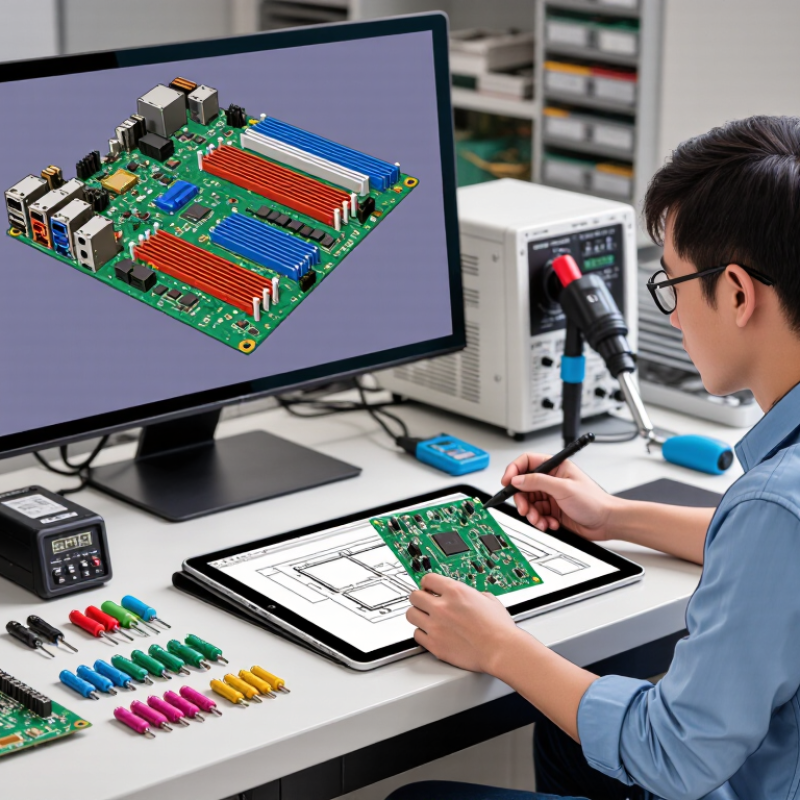
What Is a PCB Design Course?

What a PCB Design Course Covers

A PCB design course teaches how to turn an electrical schematic into a board that can be manufactured and assembled. Learners identify components, choose footprints, and arrange parts around connectors, mounting holes, and heat-sensitive devices. They then draw copper traces across one or more board layers. Small details matter: a connector placed too close to an edge can complicate assembly.

Courses commonly cover design rules, trace width, clearances, ground planes, and basic signal integrity. Students use these principles to check spacing and catch errors before production. They also learn to prepare manufacturing files, such as Gerber data and drill files. IPC standards often inform these checks, though course depth and software tools vary.

The commercial context is substantial. Grand View Research valued the global PCB market at USD 73.1 billion in 2023 and forecast a 5.7% compound annual growth rate from 2024 to 2030. A course may therefore include practical projects, such as laying out a small sensor board and reviewing its fabrication constraints. Debugging is part of the work. The first routing attempt may be messy, and passing automated checks does not guarantee an elegant or reliable design.
What Is a PCB Design Course? — What a PCB Design Course Covers

Example 40-hour course plan showing how instruction time might be distributed across core PCB design topics. The hours are illustrative, not a survey of course providers.

Core Concepts and Design Tools Taught

A PCB design course teaches how electrical ideas become manufacturable circuit boards. Students typically begin with schematic capture, component selection, and footprint creation. They then arrange parts, route copper traces, and check clearances. A useful course explains why power paths need enough copper and why high-speed signals require controlled impedance. Small errors matter. A misplaced connector can force a costly layout revision.

Design tools support each stage: schematic editors, board-layout software, simulation features, and rule-checking tools. Learners practice electrical-rule checks and design-rule checks, then prepare fabrication files such as Gerber data and drill files. They also review stackups, solder masks, and bills of materials. Grand View Research’s PCB market report estimated global market revenue at US$72.4 billion in 2023, with projected annual growth of 5.6% from 2024 to 2030. That expanding market makes practical design skills relevant, but a clean screen layout does not guarantee a reliable board. Courses should include peer review and manufacturing feedback. I still find that beginners often trust automated checks too much; they catch rule violations, not every engineering judgment.

How Students Progress Through the Design Process

A PCB design course teaches students to turn a circuit diagram into a manufacturable board. The learning path is practical: define electrical requirements, choose components, draw the schematic, then arrange parts on a board. Students learn why a capacitor belongs close to a power pin and how a narrow trace can create a problem. Small errors matter. They review design rules, route signals, and inspect clearances before generating fabrication files.

Progress is rarely a straight line. A first layout may fit on screen but fail a clearance check or make a connector awkward to reach. Students then revise, compare trade-offs, and document why they changed a trace or component position. This reflects real engineering work, where testing and correction matter as much as the initial plan. The U.S. Bureau of Labor Statistics projects 7% employment growth for electrical and electronics engineers from 2023 to 2033, with about 17,800 openings annually. Its Occupational Outlook Handbook offers broad career context, not a PCB-specific forecast.

Tips: Begin with a small board, such as a sensor circuit. Check the schematic before routing, and keep a short change log. Ask a peer to inspect connector access and ground paths. One detail may still be easy to miss. That is part of learning.

Practical Projects and Skills Development

A PCB design course is most valuable when learners build something they can inspect and test. A small sensor board, for example, can teach schematic capture, component selection, and board layout in one project. Students place parts, route copper traces, and check whether connections match the circuit diagram. They also learn why power and ground paths need careful attention. Small errors matter.

Practical work should move from simple exercises to a complete prototype. Learners might begin with a basic LED circuit, then add a connector, mounting holes, and a protective enclosure. Before fabrication, they can run design-rule checks and review clearances around pads and traces. These checks catch common problems, but they do not replace careful review. A board can pass every check and still be awkward to assemble.

Testing develops judgment that software alone cannot provide. Students can use a multimeter to check continuity, inspect solder joints, and compare measured voltages with expected values. When a circuit fails, tracing the signal path helps them find the cause instead of changing parts at random. Some first layouts need a second revision. That is normal, though it can be frustrating. Keeping notes about each change helps learners explain their decisions and improve the next design.

What Is a PCB Design Course? — Practical Projects and Skills Development
Course Module Typical Time Practical Project or Exercise Skills Developed Tangible Outcome
PCB Design Foundations 4 hours Identify board layers, components, pads, traces, and common PCB symbols. PCB terminology, schematic reading, basic component recognition A labeled board-layout worksheet
Schematic Capture 6 hours Create a simple LED indicator circuit with a resistor, connector, and power input. Component selection, symbol placement, net naming, electrical-rule checking A checked schematic and bill of materials
Board Layout and Footprints 8 hours Transfer the LED circuit to a two-layer board and place components for practical assembly. Footprint selection, board outlines, placement, design-rule setup A dimensioned PCB layout
Routing and Grounding 8 hours Route signal and power connections, add a ground plane, and review return paths. Trace-width selection, via use, ground-plane design, routing strategy A routed board that passes design-rule checks
Manufacturing Considerations 5 hours Review clearance, hole sizes, copper spacing, solder mask, and silkscreen details. Design for manufacturability, tolerance awareness, fabrication documentation A fabrication-ready design review checklist
PCB Verification and Output 5 hours Inspect the finished design in 2D and 3D, then prepare manufacturing output files. Final design review, error correction, Gerber and drill-file preparation A verified output package and assembly drawing
Capstone: Sensor Interface Board 12 hours Design a small board connecting a sensor, power input, and microcontroller header. End-to-end design workflow, documentation, troubleshooting, project planning A complete schematic, board layout, bill of materials, and design presentation
Typical Course Total 48 hours of guided instruction and practical design work

Course Formats, Prerequisites, and Learning Outcomes

What Is a PCB Design Course?
Course Formats, Prerequisites, and Learning Outcomes

A PCB design course teaches how to turn an electronic schematic into a physical circuit board. Formats vary. Classroom courses offer guided lab time, while online courses may use recorded lessons and design exercises. Hybrid options combine instruction with scheduled reviews. Check whether the course includes practical feedback, not just software demonstrations.

Most beginners benefit from basic electronics knowledge, including voltage, current, and common components. Reading simple schematics helps, but advanced engineering experience is rarely required. A computer and steady practice matter more than a perfect starting skill set. Some courses move quickly, so learners may need extra time to understand unfamiliar terms.

By the end, students may be able to create schematics, select component footprints, arrange parts, and route copper traces. They often learn design-rule checks and how to prepare manufacturing files, such as Gerber and drill data. These outcomes depend on course depth. A short course may introduce signal integrity without making students experts. Mistakes are instructive. A first layout can still feel crowded, and that is worth reviewing carefully before calling it finished.